The core of modern PCB design lies in efficiency, scalability, and modularity. Driven by the IoT boom alongside advancements in consumer electronics and industrial control technologies, there is a growing market demand for flexibly designed and easily assembled devices. It is precisely within this context that castellated hole technology (also referred to as PCB castellation or semi-plated holes) has emerged, bringing transformative changes to every stage from prototyping to mass production.
Castellations have transformed how engineers mount one PCB onto another.The castellated hole process now enables direct soldering of modules onto the main PCB or larger printed circuit board, replacing traditional interconnection methods relying on connectors and wires. This innovation fundamentally streamlines the assembly process while enhancing the efficiency and reliability of surface mounting. In high-volume manufacturing and complex PCB layouts - such as those found in Raspberry Pi Pico or custom wireless communication modules - adopting castellated holes not only facilitates rapid development but also ensures stable electrical connections and mechanical robustness.
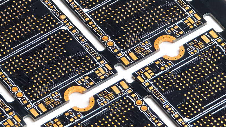
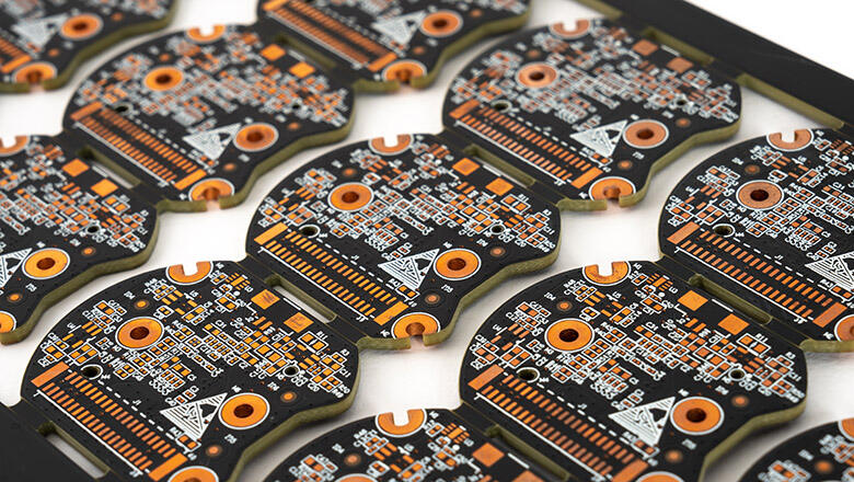
A castellated hole is a unique, semi-circular via that's partially exposed along the edge of a PCB. These holes are typically plated through-holes that, through CNC milling or routing, are sliced so that only half of the hole remains, exposed at the board’s edge. This creates what’s commonly called a half-hole, half-plated hole, semi-plated hole, or half-cut hole.
Castellations allow a module to act like a large, surface mount device. The module is designed with holes along its edge (often matching the standard pitch of plated through-holes), and these holes are then soldered onto pads on the main board—perfectly aligning sub-circuits for seamless integration.
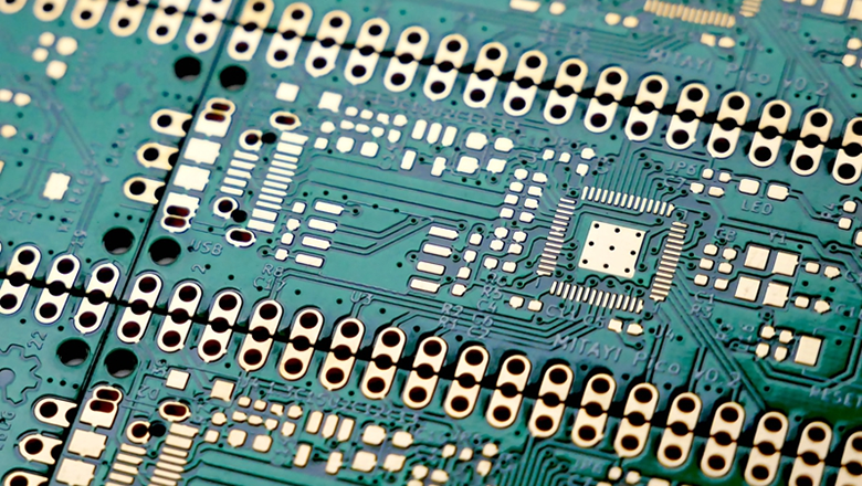
The use of castellations marks a significant evolution in PCB assembly process and module-based product design. In the field of electronic interconnection technology, early solutions were heavily reliant on through-hole components and large connectors. Today, driven by the strong trends of miniaturization and modularity, more efficient solutions are continuously advancing.
PCB castellation can be tailored for various mounting and assembly needs:
These are plated through-holes that are cut exactly in half, used along the edge of a PCB. They provide robust mechanical support and maximum electrical contact, commonly found in power modules and industrial PCBs.
Sometimes, only a section of the via is exposed at the edge, known as a partial hole. This approach is used when layout constraints or the number of connections dictate space-saving techniques without sacrificing electrical connectivity.
A zigzag or alternating pattern of holes, often used in HDI circuit boards or when there’s a need to increase the pin density along the edge. This technique is essential in communication PCBs, or for breakout boards with multiple signal types.
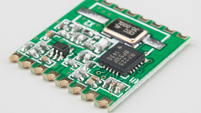
The key parameters of castellated holes (quantity, spacing, arrangement) are not fixed but are determined by the design specifications of the final application.
Most commonly, a single row of castellated holes is aligned along the edge of the module. The number of holes depends on the functions needed—more pins for complex processes, fewer for simple breakouts.
Staggered or double-row castellated hole layouts optimize grounding references and signal paths, providing fundamental assurance for the integrity of high-speed signals (such as USB, HDMI, and RF). This represents a core design methodology for enhancing the performance of high-end circuit boards.
In addition to castellated holes, standard mounting holes (unplated or fully plated) may be included for additional mechanical retention, particularly for modules handling vibration or physical stresses in industrial or automotive environments.
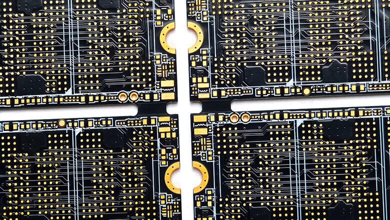
Manufacturing high-quality castellated holes on PCBs involves several specialized PCB fabrication steps:
Manufacturing Table Example:
Step |
Detail |
Drill Holes |
Holes located at board edge or periphery for castellation |
Copper Plate |
Vias and half-holes are copper-plated to ensure proper electrical path |
CNC Mill Edge |
Boards cut to expose semi-plated holes; creates distinct castellated edge |
Inspect & Clean |
Ensure no copper burrs remain; check annular ring and alignment quality |
Finish & Mask |
Solder mask applied with clearance; inspect for proper exposure |
Final Inspection |
Visual/X-ray QC for incomplete plating, burrs, and plate adhesion |
Top-quality PCB design and reliable module-to-main-board assembly depend on adhering to proven design guidelines for castellated holes in PCB projects:
The variety of applications for castellated holes and PCB castellation is staggering, reaching far beyond hobbyist boards:
While castellated holes enable modularity and fast integration, they introduce specific considerations:
Feature |
Castellated Hole(s) |
Plated Through-Holes |
Connection Type |
Surface-mount, along the board edge |
Through the board |
Application |
PCB modules, sub-circuits, breakout boards |
Headers, pins, large currents |
Miniaturization |
Excellent |
Limited by header/pin size |
Soldering Compatibility |
SMT/refow or manual |
PTH/hand/manual/automated |
Repair/Upgrade |
Easy module swap |
Pins may require desoldering |
Cost (Unit) |
Higher (special plate & milling) |
Standard PCB price |
Mechanical Robustness |
Good with extra support |
Very good |
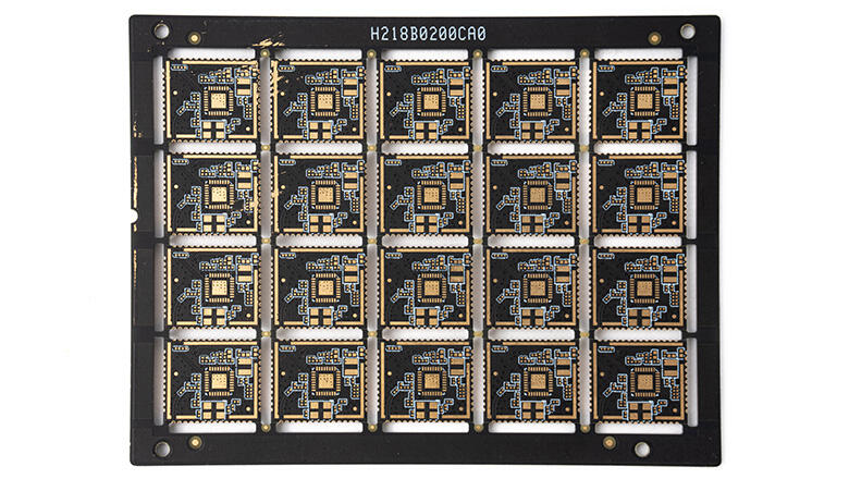
While PCB castellation incurs slightly higher unit pricing from extra CNC milling and finishing, its advantages in modularity, speed of assembly, and main PCB real estate savings far outweigh initial costs—especially as sub-circuits can be mass-produced. The assembly process is also dramatically shortened, since mounting holes and connectors are reduced or eliminated altogether.
In the PCB industry, increasing numbers of communication modules, consumer electronics, and IoT devices rely on castellation for fast “plug-and-play” product launches and easy version control of firmware or hardware. Many PCB board houses now offer special castellation services for prototyping and volume fabrication, making this technique accessible to both startups and enterprise-level teams.
Q: Can castellated holes be used for high-power signals?
A: For low-to-moderate current applications, castellated holes suffice; for high current (2A), supplement with plated through-hole or edge-plated pads.
Q: What PCB design tool supports castellation?
A: All major EDA/PCB design platforms (Altium, Eagle, KiCad, etc.) can lay out semi-plated holes and board edges; use mechanical-layer drawings for precision.
Q: Should I use castellation or headers for PCB module mounting?
A: Choose castellation when space is limited, miniaturization is critical, or for SMT-based assembly lines. Use headers for easy hand-assembly or repeated mating/unmating.
Q: How many holes should a module have?
A: The number of holes depends on signal and power/GND needs; always follow proper spacing and IPC design guidelines for reliability.
Q: Are castellation designs suitable for consumer and industrial electronics?
A: Absolutely—high-end consumer electronics, industrial control systems, and even wireless communication modules increasingly use castellated edges for robust integration.
As an innovative interconnection technology, PCB castellated holes combine the compactness of surface-mount design with the robustness of plated through-holes, providing engineers with a mature and reliable flexible solution. This excellence in module installation, functional expansion, and manufacturable sub-circuit production has established it as an exemplary process driving rapid development in IoT, modular devices, and consumer electronics.