High Frequency PCB Assembly: Advanced Solutions for Superior RF Performance

All Categories

high frequency pcb assembly

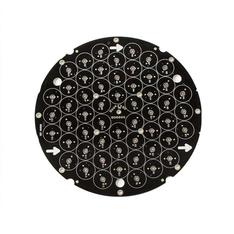
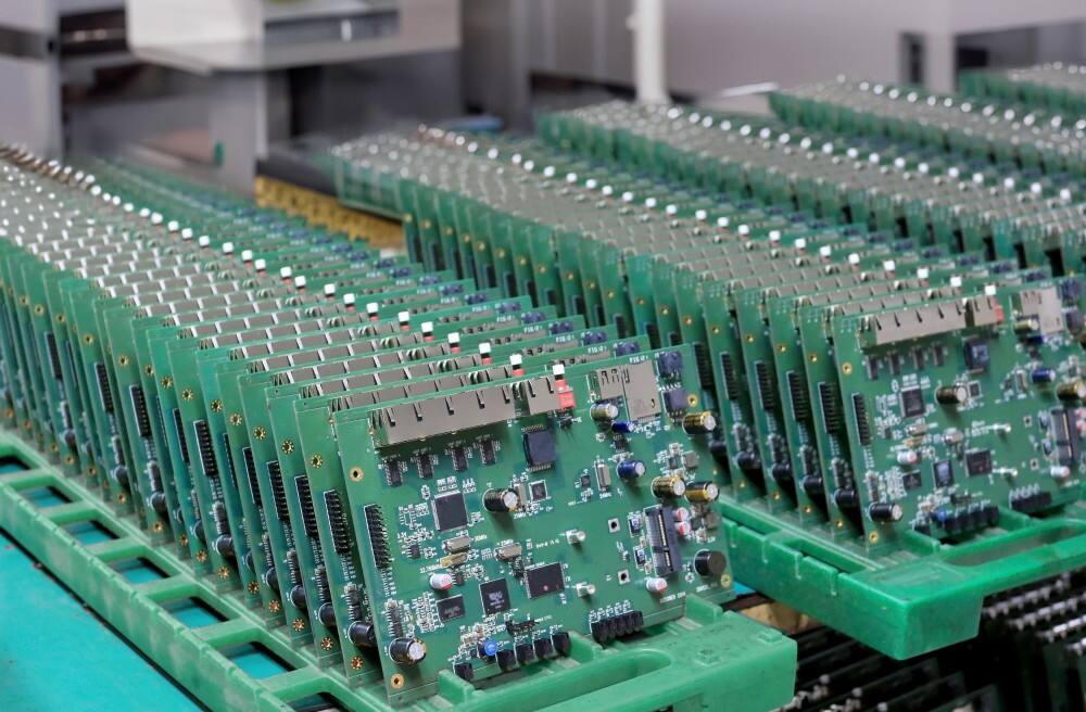
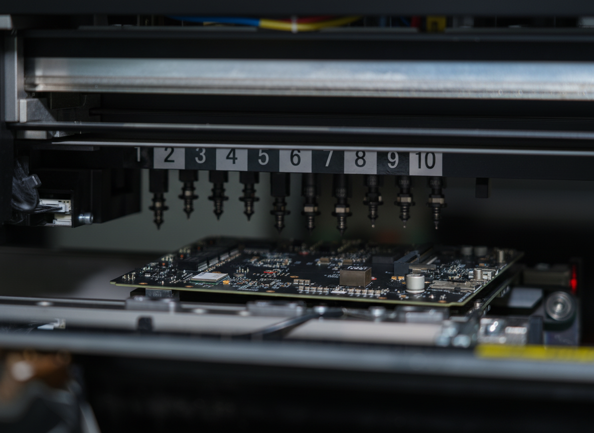
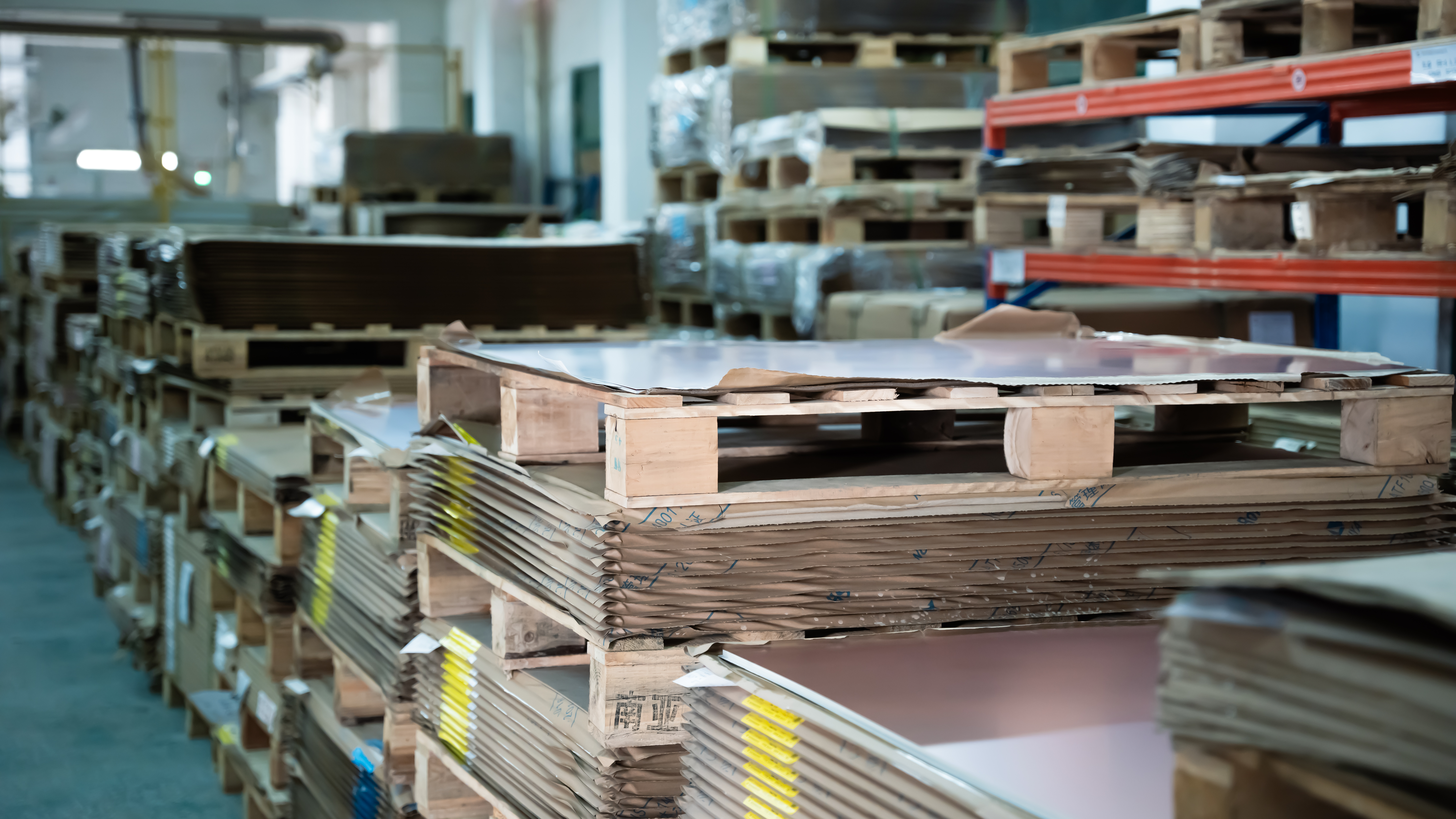
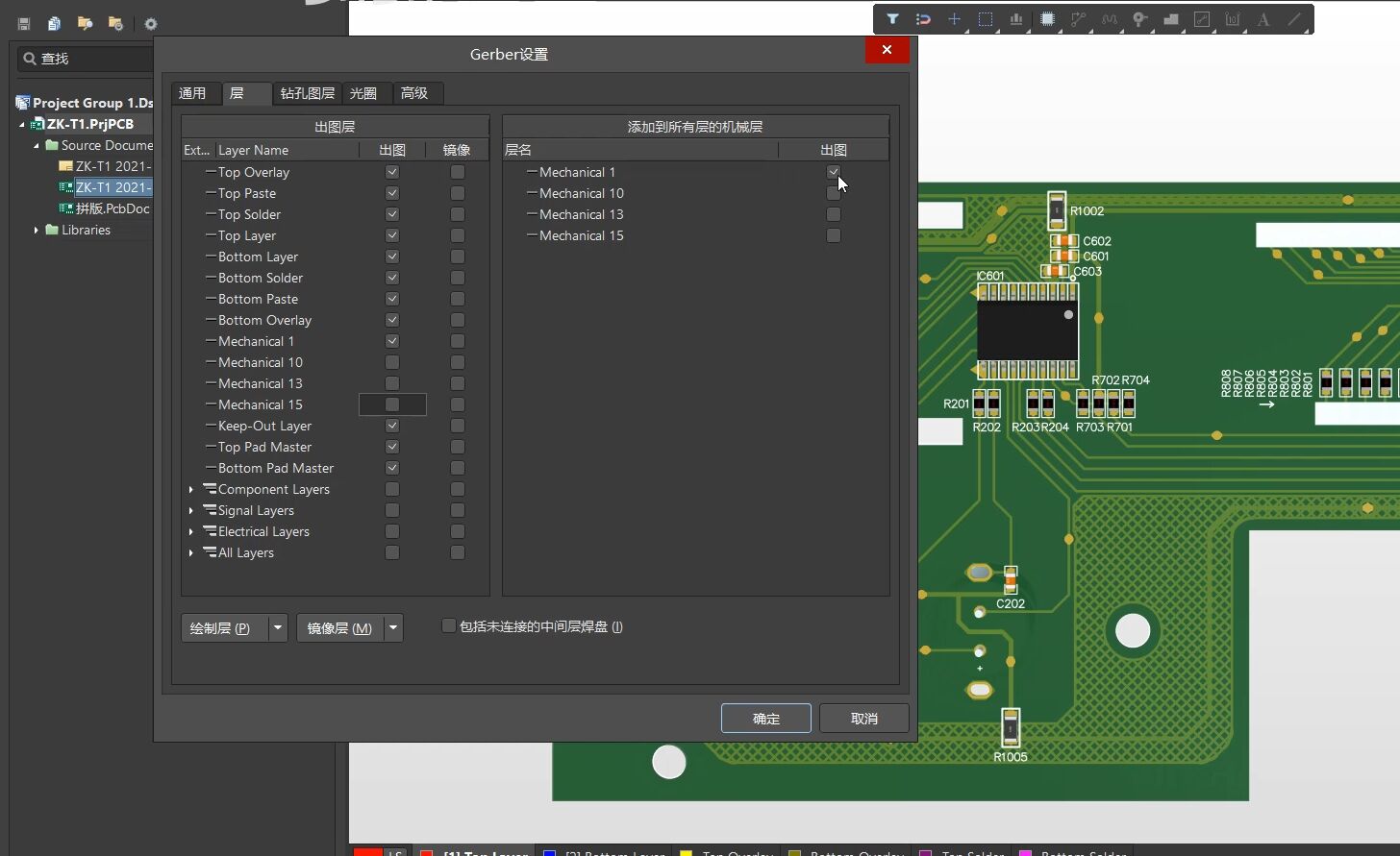
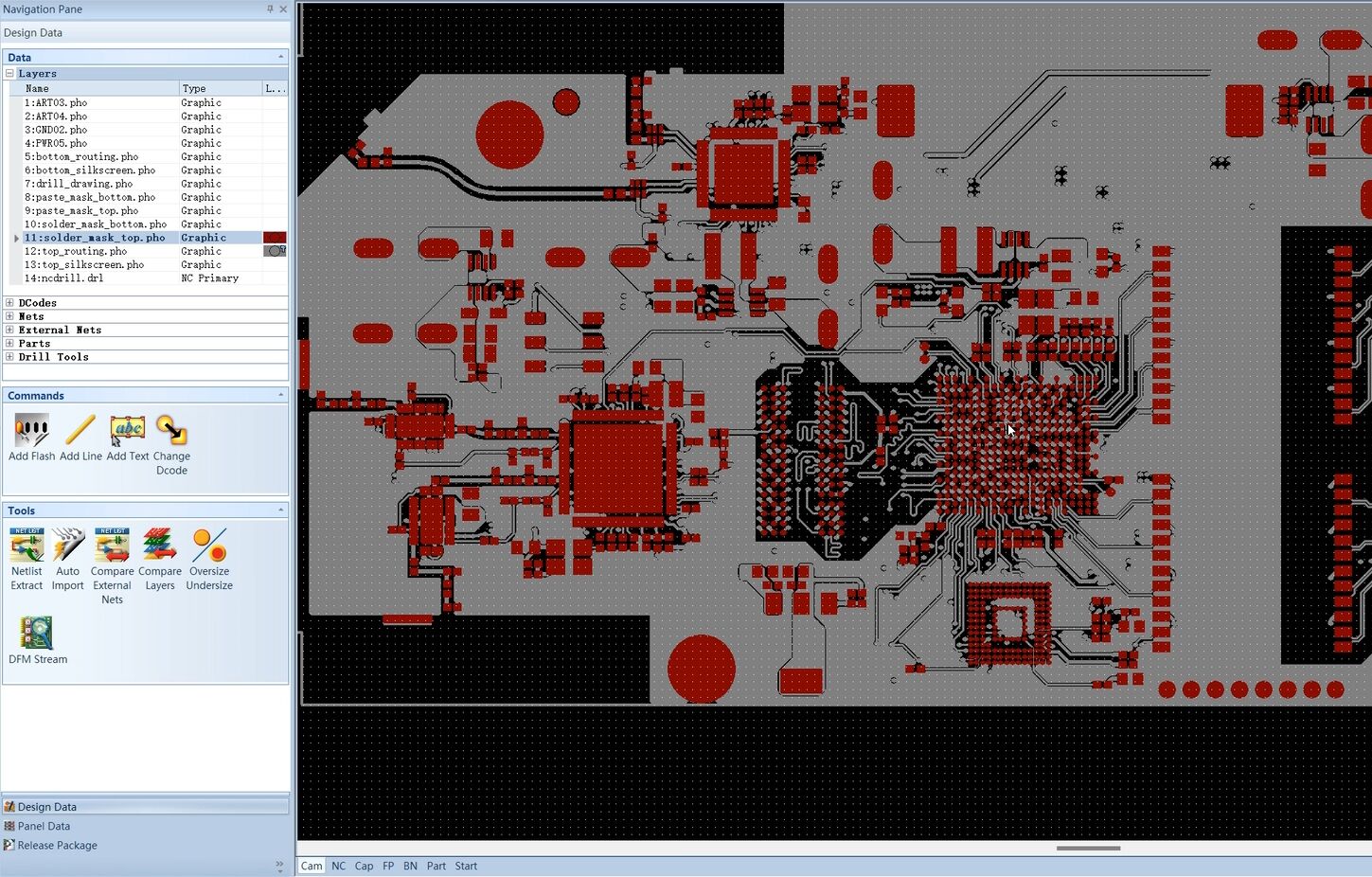
High frequency PCB assembly represents a sophisticated manufacturing process specifically designed for electronic circuits operating at frequencies above 100 MHz. This specialized assembly technique incorporates advanced materials and precise manufacturing methods to ensure optimal performance in high frequency applications. The process involves careful consideration of impedance control, signal integrity, and electromagnetic interference (EMI) shielding. These assemblies typically utilize special substrate materials like Rogers, Taconic, or high grade FR4, which offer superior electrical properties at high frequencies. The manufacturing process demands extreme precision in trace width control, spacing requirements, and layer stackup to maintain signal integrity. Key features include controlled impedance transmission lines, minimized crosstalk between signal paths, and careful attention to ground plane continuity. Applications span across various industries, including telecommunications equipment, radar systems, wireless devices, high speed digital systems, and RF/microwave equipment. The assembly process also incorporates specialized components designed for high frequency operation, such as surface mount devices (SMDs) with minimal parasitic effects and optimized lead lengths. Quality control measures include advanced testing procedures using vector network analyzers and time domain reflectometry to ensure proper functionality at the intended operating frequencies.

New Product Recommendations

High frequency PCB assembly offers numerous compelling advantages that make it essential for modern electronic applications. First, these assemblies provide superior signal integrity at high frequencies, ensuring clean signal transmission with minimal distortion or loss. This results in improved system performance and reliability. The careful material selection and manufacturing processes lead to reduced signal attenuation, enabling longer transmission distances while maintaining signal quality. Another significant advantage is the enhanced EMI shielding capabilities, which protect sensitive circuits from external interference and prevent signal leakage. The precise impedance control achieved through high frequency PCB assembly ensures optimal power transfer and minimizes signal reflections, leading to better system efficiency. These assemblies also offer excellent thermal management properties, crucial for high power RF applications. The use of specialized materials and construction techniques results in improved dimensional stability across varying environmental conditions, ensuring consistent performance. From a manufacturing perspective, high frequency PCB assemblies often feature higher component density capabilities, allowing for more compact designs without compromising performance. The assemblies demonstrate superior reliability in demanding applications, with reduced susceptibility to environmental factors such as temperature variations and humidity. Additionally, the careful attention to ground plane design and power distribution networks results in improved power integrity and reduced noise in the system. The standardized manufacturing processes ensure repeatability and consistency in production, while the advanced testing procedures guarantee performance meets specifications.

Tips And Tricks

What Are the Different Types of PCBs and Their Applications?

09

Oct

What Are the Different Types of PCBs and Their Applications?

Understanding Modern Printed Circuit Board Varieties Printed Circuit Boards (PCBs) form the backbone of modern electronics, serving as the foundation for countless devices we use daily. From smartphones to industrial machinery, different types of PCB...
View More
Why Choose PCB Solutions for Industrial Applications?

09

Oct

Why Choose PCB Solutions for Industrial Applications?

The Evolution of PCB Solutions in Modern Industrial Landscapes The industrial sector has witnessed a remarkable transformation with the integration of advanced PCB solutions into its core operations. From automated manufacturing facilities to sophist...
View More
How Are PCBs Manufactured? Key Steps and Processes Explained

09

Oct

How Are PCBs Manufactured? Key Steps and Processes Explained

Understanding the Complex Journey of Circuit Board Production PCB manufacturing has revolutionized the electronics industry, enabling the creation of increasingly sophisticated devices that power our modern world. From smartphones to medical equipmen...
View More
Why Choose Professional PCB Manufacturing Services?

09

Oct

Why Choose Professional PCB Manufacturing Services?

The Critical Role of Expert PCB Production in Modern Electronics In today's rapidly evolving electronics industry, the quality and reliability of printed circuit boards (PCBs) have become more crucial than ever. Professional PCB manufacturing service...
View More

Get a Free Quote

Our representative will contact you soon.
Email
Name
Company Name
Message
0/1000

high frequency pcb assembly

Advanced Material Technology

Advanced Material Technology

High frequency PCB assembly employs cutting edge material technologies that set it apart from conventional PCB manufacturing. The selection of substrate materials is crucial, with options like Rogers and Taconic materials offering superior dielectric properties essential for high frequency operation. These materials maintain stable electrical characteristics across wide frequency ranges and temperature variations, ensuring consistent performance. The specialized laminates feature low loss tangent values, minimizing signal attenuation and maintaining signal integrity even at extremely high frequencies. The materials also exhibit excellent dimensional stability, crucial for maintaining precise impedance control and preventing delamination under thermal stress. Advanced surface finishes are utilized to enhance conductivity and reduce skin effect losses at high frequencies. The combination of these materials with precision manufacturing techniques results in assemblies capable of supporting applications up to millimeter wave frequencies.
Precision Manufacturing Process

Precision Manufacturing Process

The manufacturing process for high frequency PCB assembly represents the pinnacle of precision engineering in electronics manufacturing. Every aspect of the process is tightly controlled to maintain critical dimensions and electrical properties. The process begins with highly accurate artwork generation and sophisticated photolithography techniques to achieve precise trace geometries. Advanced drilling and plating processes ensure via holes maintain consistent impedance characteristics. The layer registration process utilizes state of the art equipment to maintain tight tolerances essential for multilayer builds. Surface mount assembly employs precision placement equipment capable of achieving placement accuracies down to microns. Specialized reflow profiles are developed to ensure optimal soldering while maintaining the integrity of high frequency materials. The entire process is monitored through advanced inspection systems, including automated optical inspection and X ray inspection, to verify critical dimensions and assembly quality.
Comprehensive Testing and Validation

Comprehensive Testing and Validation

High frequency PCB assembly incorporates extensive testing and validation procedures to ensure performance meets specifications. The testing process begins with automated electrical testing to verify basic connectivity and shorts. Advanced vector network analyzers are employed to measure scattering parameters, providing detailed information about signal transmission characteristics and impedance matching. Time domain reflectometry testing helps identify impedance discontinuities and verify signal integrity. Environmental testing validates performance across temperature and humidity ranges. Signal integrity testing includes eye diagram analysis and jitter measurements for digital applications. EMI/EMC testing verifies compliance with regulatory requirements and confirms proper shielding effectiveness. Each assembly undergoes rigorous quality control procedures, including dimensional verification and surface inspection. The comprehensive testing approach ensures reliable performance in demanding high frequency applications.
High Frequency PCB Assembly: Advanced Solutions for Superior RF Performance

Get a Free Quote

Our representative will contact you soon.
Email
Name
Company Name
Message
0/1000