High frequency PCB designs have become indispensable in modern radio frequency applications, where signal integrity and minimal loss are paramount. As wireless communication systems, radar technologies, and satellite networks continue to evolve, the demand for circuit boards capable of handling frequencies from several hundred megahertz to multiple gigahertz has intensified dramatically. Understanding what makes high frequency PCB constructions particularly suited for RF work requires examining their unique material properties, design characteristics, and performance advantages that conventional circuit boards simply cannot match in these demanding environments.
The fundamental distinction between standard PCB technology and high frequency variants lies in how they manage electromagnetic energy at elevated frequencies. While traditional circuit boards excel at lower frequency applications, RF environments introduce challenges such as signal attenuation, dielectric losses, impedance mismatches, and electromagnetic interference that require specialized engineering solutions. High frequency PCB platforms address these challenges through carefully selected substrate materials, precise impedance control, and design methodologies that preserve signal fidelity across the entire frequency spectrum where RF systems operate.
Material Properties That Enable RF Performance
Low Dielectric Constant for Signal Propagation
The dielectric constant of a PCB substrate fundamentally determines how electromagnetic waves propagate through the board material. High frequency PCB constructions utilize specialized laminates with dielectric constants typically ranging from 2.2 to 4.5, significantly lower than the 4.2 to 4.8 range found in standard FR-4 materials. This lower dielectric constant reduces signal propagation delay and minimizes the capacitance between conductors, which becomes critically important as operating frequencies increase into the gigahertz range. Materials such as Rogers, Taconic, and PTFE-based laminates provide these optimal dielectric properties while maintaining stability across temperature variations.
The impact of dielectric constant on RF performance extends beyond simple signal speed considerations. Lower dielectric values reduce the physical size requirements for transmission line structures, allowing more compact circuit designs without sacrificing electrical performance. This becomes particularly advantageous in modern RF applications where miniaturization pressures demand increasingly dense component placement. Additionally, materials with consistent dielectric properties across frequency ranges ensure predictable circuit behavior, eliminating the performance drift that can plague RF systems built on conventional PCB substrates as operating frequencies change.
Minimal Dissipation Factor for Energy Efficiency
The dissipation factor, also known as loss tangent, measures how much electromagnetic energy a PCB material converts to heat rather than transmitting it through the circuit. High frequency PCB materials feature exceptionally low dissipation factors, often below 0.002, compared to standard PCB materials that typically exhibit values above 0.02. This dramatic reduction in dielectric loss becomes increasingly critical as frequency rises, since insertion loss increases proportionally with both frequency and dissipation factor. For RF applications operating in the microwave spectrum, even small improvements in dissipation factor translate to measurably better signal transmission efficiency.
Material selection based on dissipation factor directly influences system performance parameters that matter to RF engineers. Lower loss tangent values enable longer transmission line runs without requiring signal amplification, reduce thermal management requirements, and improve overall system power efficiency. In applications such as phased array antennas, satellite communications, and 5G infrastructure, where signals may traverse multiple PCB layers and interconnects, the cumulative effect of low-loss materials becomes the difference between meeting specifications and system failure. Advanced high frequency PCB materials maintain their low dissipation characteristics even under temperature extremes and humidity exposure.
Thermal Stability for Consistent Operation
Thermal stability represents another critical material property that distinguishes high frequency PCB platforms from conventional alternatives. RF circuits generate heat during operation, and ambient temperature variations in deployment environments can span from subzero to extreme high temperatures. High frequency PCB materials exhibit minimal changes in dielectric constant and dissipation factor across these temperature ranges, ensuring that impedance characteristics and signal integrity remain stable regardless of thermal conditions. This stability prevents frequency drift, maintains filter response characteristics, and preserves amplifier matching networks under real-world operating conditions.
The coefficient of thermal expansion in high frequency PCB laminates also plays a vital role in maintaining reliability. Materials with expansion coefficients closely matched to copper conductors minimize mechanical stress during temperature cycling, reducing the risk of via barrel cracking, pad delamination, and solder joint failure. For RF applications in aerospace, automotive radar, and outdoor telecommunications equipment, where temperature cycling is inevitable, this thermal mechanical stability extends product lifespan and reduces field failures. Advanced laminate systems incorporate glass reinforcement structures that provide dimensional stability while maintaining the electrical properties essential for RF performance.
Design Characteristics Optimized for RF Transmission
Controlled Impedance for Signal Integrity
Impedance control stands as perhaps the most fundamental design requirement for high frequency PCB applications in RF systems. Unlike lower frequency circuits where impedance variations may be tolerable, RF transmission lines must maintain precise characteristic impedance values, typically 50 or 75 ohms, throughout the signal path. High frequency PCB manufacturing processes incorporate tight tolerances on trace width, substrate thickness, and dielectric constant to achieve impedance control within ±10% or tighter. This precision prevents signal reflections that would otherwise degrade RF performance through standing waves, return loss, and reduced power transfer efficiency.
The geometry of transmission line structures on high frequency PCB platforms requires careful engineering to achieve and maintain target impedance values. Microstrip, stripline, and coplanar waveguide configurations each offer specific advantages depending on frequency range, isolation requirements, and circuit topology. Advanced PCB design software employs electromagnetic field solvers to model these structures accurately, accounting for factors such as copper roughness, dielectric thickness variations, and conductor edge effects that become significant at RF frequencies. Proper ground plane implementation, via placement strategies, and return path continuity all contribute to maintaining controlled impedance throughout complex RF circuit layouts.
Minimized Conductor Losses Through Surface Treatment
Conductor losses in high frequency PCB designs arise from two primary mechanisms: DC resistance and skin effect at elevated frequencies. As frequency increases, current tends to flow primarily on the surface of conductors rather than through their entire cross-section, a phenomenon that effectively increases resistance. High frequency PCB fabrication addresses this challenge through several approaches, including heavier copper weights to increase surface area, smooth copper foil treatments to reduce surface roughness effects, and specialized plating processes that optimize conductivity. Some advanced designs employ silver or gold plating on critical RF traces to further minimize resistive losses.
The impact of surface roughness on high frequency PCB conductor loss has gained increasing attention as operating frequencies push higher. Traditional copper foil features a rough profile designed to enhance adhesion to laminate materials, but this roughness increases effective path length for high frequency currents traveling along the surface. Manufacturers now offer low-profile copper foils and surface treatments specifically engineered for RF applications, reducing conductor losses by significant margins compared to standard copper. In applications where every fraction of a decibel matters, such as satellite transponders or base station power amplifiers, these conductor optimization techniques contribute measurably to overall system performance.
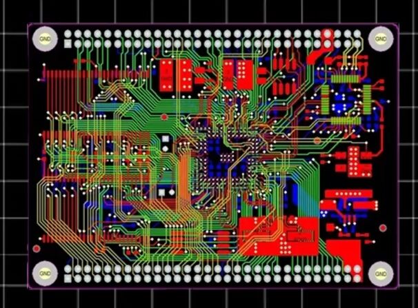
Layer Stack-Up Architecture for Isolation and Routing
The layer stack-up architecture in high frequency PCB designs profoundly influences RF performance through its impact on crosstalk, electromagnetic interference, and signal routing flexibility. Multi-layer high frequency PCB constructions typically incorporate dedicated ground planes that provide low-impedance return paths for RF currents and electromagnetic shielding between signal layers. Strategic placement of power and ground planes creates natural barriers that isolate sensitive RF circuits from noisy digital sections, a critical consideration in modern mixed-signal RF systems where microprocessors and data converters coexist with sensitive receiver front-ends.
Advanced high frequency PCB stack-ups employ asymmetric layer configurations when needed to accommodate different impedance requirements on various layers. For example, a four-layer RF PCB might feature thin dielectric spacing between the top signal layer and the first ground plane to achieve 50-ohm microstrip impedance, while using thicker dielectric between internal layers for 75-ohm stripline structures. Via design within these stack-ups requires special attention, as discontinuities introduced by layer transitions can create impedance bumps that reflect RF energy. Blind and buried via technologies, back-drilling techniques, and via fence structures all represent specialized PCB fabrication capabilities that enhance RF performance in complex multi-layer designs.
Performance Advantages in Demanding RF Environments
Superior Signal Fidelity Across Wide Bandwidths
High frequency PCB platforms deliver exceptional signal fidelity that proves essential for wideband RF applications where signal quality directly determines system capability. The combination of low dielectric loss, controlled impedance, and minimal dispersion allows these circuit boards to transmit complex modulated signals with minimal distortion across bandwidths spanning multiple octaves. This performance becomes critical in applications such as software-defined radio, wideband electronic warfare systems, and modern cellular infrastructure supporting multiple frequency bands simultaneously. Conventional PCB materials would introduce amplitude and phase distortions that corrupt signal integrity in these demanding applications.
The flat frequency response characteristic of properly designed high frequency PCB circuits ensures that all spectral components of a signal experience similar propagation delays and attenuation. This property preserves the time-domain characteristics of digital modulation schemes and prevents inter-symbol interference that would otherwise increase bit error rates. For high-speed data transmission over RF links, where spectral efficiency demands complex modulation formats like 64-QAM or 256-QAM, the superior signal fidelity of high frequency PCB implementations directly translates to higher achievable data rates and more robust link margins. Testing and validation of these characteristics requires vector network analysis across the entire operating bandwidth to verify performance margins.
Reduced Electromagnetic Interference and Emissions
Electromagnetic compatibility represents a constant challenge in RF system design, and high frequency PCB constructions offer inherent advantages in controlling both radiated emissions and susceptibility to external interference. The combination of proper grounding techniques, controlled impedance transmission lines, and strategic shielding plane placement creates a circuit board environment that naturally contains electromagnetic energy within intended paths. This containment reduces unintentional radiation that could interfere with nearby circuits or violate regulatory emission limits, while simultaneously improving immunity to external interference sources that might otherwise couple into sensitive receiver circuits.
Advanced high frequency PCB designs incorporate electromagnetic interference mitigation strategies that go beyond simple shielding. Differential signaling techniques, guard trace implementations, and via stitching patterns all contribute to creating a low-EMI circuit environment. For RF applications in densely populated equipment racks or mobile devices where multiple wireless systems operate in close proximity, these EMI control techniques prevent cross-coupling that would otherwise degrade receiver sensitivity or create spurious transmitter emissions. Electromagnetic simulation during the design phase allows engineers to identify and address potential EMI issues before committing to PCB fabrication, saving costly redesign cycles.
Enhanced Power Handling Capability
Power handling represents a critical performance parameter for RF applications involving transmission systems, where high frequency PCB designs must safely conduct and dissipate significant RF power levels. The thermal conductivity of specialized PCB laminates, combined with appropriate copper weight selection and thermal via implementation, enables effective heat removal from power amplifier stages and other high-dissipation components. Some high frequency PCB constructions incorporate metal-core or ceramic substrates that provide thermal conductivity orders of magnitude higher than standard epoxy-glass materials, enabling power densities that would cause conventional PCB designs to fail thermally.
Beyond thermal considerations, the electrical characteristics of high frequency PCB platforms directly influence power handling through voltage breakdown resistance and current carrying capacity. High-quality RF laminates maintain their dielectric integrity under the high electric field strengths present in power amplifier output stages, preventing corona discharge or dielectric breakdown that could catastrophically damage circuits. Wide, low-impedance power distribution networks fabricated with heavy copper conductors ensure adequate current delivery to power amplifiers while minimizing resistive losses that would otherwise generate waste heat. For applications such as radar transmitters, broadcast systems, and wireless infrastructure base stations, these power handling capabilities prove essential to meeting system performance requirements.
Application-Specific Requirements and Solutions
Millimeter-Wave Frequency Performance
As RF applications push into millimeter-wave frequency bands above 30 GHz for applications like 5G communications, automotive radar, and point-to-point backhaul links, high frequency PCB requirements become increasingly stringent. At these elevated frequencies, conductor losses increase due to skin effect, dielectric losses become more pronounced, and even minor impedance discontinuities create significant signal reflections. Specialized high frequency PCB materials optimized for millimeter-wave applications feature exceptionally low dissipation factors below 0.001 and extremely tight dielectric constant tolerances to maintain consistent performance. Surface roughness control becomes paramount, as the skin depth at 77 GHz automotive radar frequencies measures only a few hundred nanometers.
Manufacturing precision requirements for millimeter-wave high frequency PCB designs challenge conventional fabrication processes. Line width tolerances must tighten to ±0.5 mils or better to maintain impedance control, and substrate thickness variations must be minimized through careful material selection and pressing processes. Via design requires particular attention at millimeter-wave frequencies, where even small via stubs act as resonant structures that disrupt signal transmission. Advanced fabrication techniques such as laser-drilled microvias, sequential build-up processes, and precision depth-controlled drilling enable the high-density, low-loss interconnect structures required for successful millimeter-wave PCB implementation. Design rule checking and electromagnetic simulation become mandatory rather than optional at these frequencies.
Mixed-Signal Integration Challenges
Modern RF systems increasingly integrate analog RF circuits, high-speed digital signal processing, and power management functions onto single high frequency PCB assemblies, creating complex mixed-signal design challenges. The sensitive RF receiver front-ends must coexist with noisy switching power supplies and high-speed digital circuits generating broadband interference, all while maintaining the signal-to-noise ratios necessary for proper operation. High frequency PCB designs address these challenges through careful partitioning strategies that physically separate RF, digital, and power domains, combined with dedicated ground plane sections that prevent noise coupling between domains.
Power integrity in mixed-signal high frequency PCB designs requires special attention to prevent digital switching noise from modulating RF circuit performance. Separate power distribution networks for RF and digital sections, combined with extensive decoupling capacitor networks and ferrite bead filtering at domain boundaries, maintain clean power delivery to sensitive circuits. Clock distribution represents another critical consideration, as even low-level clock harmonics can mix with RF signals to create spurious responses that degrade receiver selectivity. Differential clock routing, spread-spectrum clocking techniques, and careful PCB trace routing all contribute to managing the electromagnetic compatibility challenges inherent in mixed-signal RF systems. Successful integration requires close collaboration between RF, digital, and PCB designers throughout the development process.
Environmental Durability and Reliability
RF applications deployed in harsh environments demand high frequency PCB constructions that maintain electrical performance while withstanding mechanical stress, temperature extremes, humidity exposure, and chemical contaminants. Aerospace and defense applications subject circuit boards to vibration profiles that would quickly fatigue conventional PCB materials, requiring specialized laminates with enhanced mechanical properties and reinforcement structures. High frequency PCB materials designed for these applications incorporate woven glass reinforcement patterns that provide mechanical strength without introducing the dielectric anisotropy that can degrade RF performance in some reinforcement schemes.
Moisture absorption represents a significant reliability concern for high frequency PCB materials, as water ingress degrades dielectric properties and creates corrosion pathways that compromise conductor integrity. Advanced RF laminates feature hydrophobic characteristics and low moisture absorption coefficients that maintain electrical stability even in high-humidity tropical environments or when exposed to condensing conditions. Conformal coating application provides an additional barrier against environmental contaminants, though coating material selection requires careful consideration to avoid introducing dielectric losses that would negate the benefits of the high-performance PCB substrate. Qualification testing for environmental durability typically includes temperature cycling, thermal shock, humidity exposure, and salt fog testing to verify that high frequency PCB assemblies will survive deployment conditions throughout their intended service life.
FAQ
What frequency range qualifies a PCB as high frequency for RF applications?
High frequency PCB classifications typically begin at frequencies above 500 MHz, though the designation relates more to wavelength relative to circuit dimensions than absolute frequency. Most RF engineers consider PCB designs operating above 1 GHz as definitely requiring high frequency considerations, while applications in the 100-500 MHz range may or may not require specialized materials depending on circuit complexity and performance requirements. The critical factor is whether signal wavelengths approach the physical dimensions of PCB traces and features, at which point transmission line effects dominate and specialized design techniques become necessary.
Can standard FR-4 PCB material work for RF applications below 2 GHz?
Standard FR-4 material can function in some RF applications below 2 GHz, particularly for non-critical circuits or where performance margins are generous, but it presents significant limitations compared to dedicated high frequency PCB laminates. FR-4's higher dissipation factor introduces more loss than optimal, its dielectric constant varies with frequency and temperature more than desired, and its material properties show broader manufacturing tolerances that complicate impedance control. For cost-sensitive consumer applications with relaxed specifications, FR-4 may prove acceptable, but professional RF designs typically employ higher-performance materials even at sub-2 GHz frequencies to ensure predictable, repeatable performance.
How does PCB thickness affect high frequency RF performance?
PCB thickness directly influences transmission line impedance calculations, with thicker substrates requiring wider traces to achieve the same characteristic impedance as thinner materials. This relationship affects circuit density and minimum feature sizes achievable in high frequency PCB layouts. Additionally, thicker PCB constructions introduce longer via lengths that create greater inductance and potential resonances at RF frequencies. For optimal RF performance, designers often specify thinner core and prepreg materials than standard PCB stack-ups, typically using dielectric thicknesses between 5 and 20 mils for controlled impedance layers, rather than the thicker build-ups common in purely digital designs.
What role does copper weight play in high frequency PCB RF performance?
Copper weight selection in high frequency PCB designs involves balancing several competing factors. Heavier copper provides lower DC resistance and can reduce skin effect losses by offering more surface area for high frequency current flow, but it also makes achieving fine trace geometries more difficult due to etching constraints and creates thicker conductors that affect impedance calculations. Most RF designs employ half-ounce or one-ounce copper for signal layers to enable fine pitch routing while maintaining acceptable conductor losses, reserving heavier copper weights for power distribution planes where resistance reduction outweighs other considerations. Ultra-high frequency applications sometimes specify even thinner copper followed by surface plating to optimize the tradeoff between conductivity and fabrication precision.