Introduction: Understanding USB, Pinouts, and PCB Design
In today's world of ubiquitous smart devices, a stable and efficient USB interface is the fundamental factor in creating successful products . Whether pursuing ultimate data transfer speeds or enabling fast, reliable charging, the underlying core relies on a deep understanding of the USB pinout and its precise implementation in both PCB design and the manufacturing process.
The core value of the USB pinout isn’t just in physical connectors—it’s in defining the rules for data transfer and power delivery between a wide range of devices. Engineers, makers, and manufacturers must have deep knowledge of USB to support accurate communication, fast file transfers, and reliable device charging. From USB 2.0 to USB Type-C and USB Power Delivery (USB PD), understanding USB pinout is at the heart of robust connectivity, high-speed USB signals, and practical designs. As a leading PCB manufacturer, pcbally engineering team notes that this deep grasp of USB pinout is also critical to addressing design challenges during production—turning circuit designs into PCB products with compliant performance and consistent quality. This aligns with pcbally key philosophy: exceptional PCB manufacturing isn’t just about processing according to drawings, but about proactively providing manufacturability feedback and process support for designs (rooted in a deep understanding of circuit principles and potential risks) to bridge innovative USB-centric designs to successful mass production, ultimately enhancing the product’s market competitiveness.

How USB Works: Theory, Interface, and Data Transfer

The Fundamentals: What is USB?
USB, short for Universal Serial Bus, is not merely a physical interface but a complete set of communication protocol standards. It defines the rules for data transfer and power delivery between a host and devices. The USB protocol defines the rules for data, including speed, transfer types, handshaking, and error correction. Within a USB interface, a host (e.g., PC, smartphone, or hub) initiates communication and controls data transfer to peripheral devices (e.g., mouse, keyboard, flash drive).
Data Transmission and Power
USB transmits data via differential pairs (e.g., D+ and D-) to combat interference, while supplying power through the VBUS pin. With technological iterations, data rates have grown exponentially—from 480 Mbps for USB 2.0 to 40 Gbps for USB4—placing extremely high demands on PCB material selection, routing precision, and impedance control. pcbally assisted a USB4 laptop client in resolving speed compliance issues. The root cause was traced to a differential pair length mismatch of 300 mils, far exceeding the 150 mils limit. After routing adjustments, signal integrity test pass rates surged from 60% to 100%.
The requirements of the USB protocol for data transfer and power delivery ultimately materialize through the pinout. Differences in speed and power across protocol versions directly dictate the evolution in pin count and functional definitions.
Key Concepts:
- USB interface: The hardware and protocol for communications and charging.
- Data transfer speed / rates: The maximum supported by a given USB standard, crucial for fast file transfer and media usage.
- Power delivery: The way USB delivers electricity, especially advanced in USB Type-C, supporting up to 100W.
Understanding USB Pinout: Essentials for PCB Design

A pinout can be understood as the "wiring diagram" for a USB connector, explicitly defining the function of each pin—data, power, ground, or control. Understanding USB pinout is vital for safe, reliable hardware.
Within a USB Pinout: Structure and Function
- Pinout consists of four pins (USB 2.0) or up to 24 (USB Type-C).
- Pins are assigned to VBUS (power), GND (ground), D+, D− (data), and extra lanes for high-speed and alternate functions.
- Pinout diagrams provide a visual reference for functional mapping.
Why Pinout Knowledge Matters
- Prevents Hardware Damage: Reversing VBUS and GND is catastrophic. Clear pinout definition is the first line of defense for hardware safety.
- Ensures Functionality: Correct connections are fundamental for device enumeration, high-speed data transfer, and fast charging.
- Enhances Manufacturability: Rational pad design helps improve the SMT yield rate and reduce defects like cold solder joints and solder bridges. Particularly for high-density connectors like Type-C, pad size and spacing must account for SMT placement accuracy and solder paste printing capability. Insufficient spacing or poor solder mask design can very easily lead to bridging.
- Precise pin mapping is paramount for PCB manufacturing to avoid catastrophic shorts or opens. A minor pin definition error in the Gerber files can scrap an entire production batch. For instance, a short between the Type-C A5/B5 (CC) pins and GND will prevent device recognition and PD negotiation. Therefore, a critical connectivity and isolation check of pin networks during pcbally front-end engineering review (DFM) is essential.
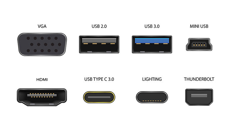
Types of USB Connectors, Cables, and Pinout Diagrams
Types of USB
Type |
Used For |
Pin Count |
Key Features |
Micro USB |
Phones, accessories, IoT |
5 |
Small, supports OTG |
Mini-USB |
Legacy, cameras |
5 |
Larger, rare in modern designs |
USB Type-A |
Hosts, computers, chargers |
4 (9 in 3.x) |
The classic rectangular plug |
USB Type-B |
Printers, industrial, devices |
4 (9 in 3.x) |
Squared plug for devices |
USB Type-C |
Everything |
24 |
Universal, reversible, PD |
Types of USB Cables
- Type-A to Type-B: Printers, older hardware.
- USB Type-C: Modern laptops, tablets, fast charging (USB-PD uses USB Type-C connectors).
- Micro-USB: Mobile devices and embedded boards.
- Type-A to Micro/Mini: Small peripherals.
- USB Type-C to Type-A: Transition cables for modern to classic hardware.

Pinout Configurations and Pinout Diagrams Explained
Pinout diagrams provide a visual, precise map for every type of connector. See below for practical diagrams and guides to understanding USB pinout:
Pin |
Signal |
Function |
Color |
1 |
VBUS |
+5V Power |
Red |
2 |
D- |
Data - |
White |
3 |
D+ |
Data + |
Green |
4 |
GND |
Ground |
Black |
Modern USB Type-C Pinout Diagram
Pin(s) |
Signal |
Function |
A1/B12 |
GND |
Return path |
A4/B9 |
VBUS |
Power source, +5 to +20V (PD supported) |
A5/B5 |
CC1/CC2 |
Orientation & power config |
A6/A7, B6/B7 |
D+/D- |
Data transmission (legacy support) |
A2/A3/B10/B11 |
SSTX/SSRX |
SuperSpeed data (USB 3.1/3.2/USB4) |
A8/B8 |
SBU1/SBU2 |
Sideband use (video/audio) |
- Understanding pinout diagrams ensures proper wiring for data transfer and power delivery in USB PCB design.
Understanding USB Pin Configurations
-
Correct USB pinout configuration prevents short circuits and enables:
- Device enumeration
- Fast charging
- High-speed USB data transfer
- Safe alternate modes (e.g., video via USB-C)
USB Standards, Data Transfer Speed, and PCB Design Impact
Different USB types and versions define transfer rates and pinout complexity:
USB Standard |
Data Transfer Rate |
Recommended Traces/PCB Design Features |
USB 1.1/2.0 |
12 / 480 Mbps |
Basic 4 pins, 90Ω diff. impedance on D+/- |
USB 3.0/3.1 |
5 / 10 Gbps |
9 pins (Type-A/B), controlled impedance, |
|
|
SuperSpeed SSRX/SSTX routing, GND shielding |
USB 3.2/USB4 |
20 / 40 Gbps |
24 pins (Type-C), symm. routing, stackup, |
|
|
strict length matching, low-loss PCB |
Data Transfer and Power Delivery in PCB Design
PCB design is deeply shaped by data rate and power requirements. In high-speed USB PCB design, layout—especially pcb component placement and pcb assembly methods—must account for differential impedance, short trace lengths, and proper ground returns.
- Data transfer speed demands matching D+/D- or SSRX±/SSTX± trace lengths within <150 mils (~4mm).
- For power delivery, wide VBUS traces and copious grounding prevent voltage drop at high current.
- Attention to USB port routing and connector selection avoids crosstalk and ensures USB data transmission integrity across different USB types.
USB Power Delivery: Accurate Transfer and Charging
USB Power Delivery (USB PD) transforms the capabilities of USB connections—particularly when paired with USB Type-C. By leveraging USB Type-C connectors, USB PD negotiates voltages ranging from 5V to 20V, delivering up to 100W of power to devices like laptops and monitors. This evolution expands USB from a mere peripheral power source into a comprehensive solution for both charging and file transfer.
Key Facts for USB PD Implementation
- Both host and device, as well as the cable, MUST support PD for higher voltage/current.
- PD negotiation takes place over CC pins in Type-C.
- USB PD also dynamically adjusts voltage based on device requirements (e.g., 5V for smartphones, 20V for laptops).
Best Practices for USB Power Delivery in PCB Design:
- Use a short, wide VBUS trace from connector to load.
- Place decoupling capacitors near VBUS pin lower ripple and noise.
- Incorporate appropriate TVS/ESD diodes at the connector entry for protection—this is especially critical for USB PCBs designed for field use (e.g., wearables, industrial devices).
- Always adhere to the official USB protocol specifications for data transfer and PD negotiation.
Choosing the Right USB Connector: Practical PCB Design Tips
Choosing the right USB connector impacts not only functionality but also PCB layout, assembly complexity, and end-product durability.
Considerations When Selecting a USB Connector
- Application and speed: Use USB Type-C for future-proofing or SuperSpeed (USB 3.x/USB4), Micro USB for legacy mobile, Type-A/Type-B for host or device.
- Mechanical stability: For high-cycle products, use connectors rated for ≥10,000 insertions.
- PCB footprint and assembly: Ensure the connector fits your PCB, supports your manufacturing method (through-hole vs. SMT), and can handle your expected current.
- EMI shielding and alignment: Especially in high-speed USB designs, a shielded, well-anchored connector improves reliable USB operation.
- Support for USB PD: Make sure the connector has the necessary CC and SBU pins for full USB power delivery features.
Best Practices for USB PCB Design, PCB Layout, and Assembly
Essential Rules for Data Transfer Integrity
- Impedance Control – For USB 2.0, D+ and D− must be routed as 90Ω differential pairs. For USB 3.x and up, all SuperSpeed pairs must follow suit.
- Short, direct traces – Keep data lines as short as possible and avoid sharp corners or long via chains.
- Matched length – Keep D+/D− (and all differential pairs) matched in length for signal integrity.
- Grounding and shielding – Use continuous ground planes under the USB interface, surround sensitive traces with ground pours or shielding stitches if possible.
- Component placement – Place ESD/TVS diodes close to the USB connector entry.
- Decoupling – Multi-value ceramic capacitors (e.g., 0.1μF, 1μF, 10μF) near VBUS, plus a bulk cap (≥22μF), minimize noise and ripple.
- Testability – Add test points for VBUS, GND, data, CC pins for easy inspection and troubleshooting during PCB assembly and production.
Troubleshooting USB Connections: Reliable USB Performance
No matter how perfect your original usb pcb design is, real-world factors can introduce usb pinout issues or affect data transfer and power delivery. Troubleshooting usb connections systematically results in faster fixes and happier users.
Common USB Connection Failures—and Solutions
Problem |
Potential Cause |
Solution |
No device detected |
Broken D+/D- trace, cold solder, wrong pinout, ESD damage. |
Inspect the USB, continuity test, Optimize ESD protection layout |
Slow data transfer |
Using wrong type of USB cable or port |
Use certified high-speed cable & port |
Unstable charging |
Undersized VBUS trace or bulk cap |
Increase VBUS width/capacitance |
Device resets randomly |
ESD, unstable power, poor ground |
Improve protection, review PCB layout |
File transfer errors |
EMI/crosstalk, impedance mismatch |
Review differential pair routing, check EMI filtering |
Troubleshooting Steps
- Visual Inspection — Are all USB pins correctly soldered? Are there bent pins, poor connections, or ESD damage on the PCB or connector?
- Check Pinout — Always reference your pinout diagram and inspect continuity for all signal and power pins.
- Swap to Known Good Cable/Port — Rule out external factors.
- Oscilloscope Verification — Examine D+/D- and SuperSpeed lanes for clarity, correct amplitude, and protocol compliance.
- Check Drivers — Sometimes, usb drivers or firmware issues can cause what seems like a hardware failure.
- Update PCB Design — For recurring issues, revisit your USB PCB design and check for impedance or grounding issues using design and test tools.
Modern USB Applications and Examples: From Theory to Practical PCB Design
From Theory to Practical PCB Design
- Wearable Health Trackers: Combine USB Type-C for both fast charging (USB PD) and accurate data transfer, using robust, waterproof connectors.
- IoT Sensors: Use Micro USB or Type-C, minimizing board size but ensuring reliable USB data transmission and power.
- Industrial USB Devices: Opt for shielded USB Type-B or ruggedized USB-C for high durability and EMI protection.
- Laptops and Tablets: Rely on high-speed USB 3.2/USB4 over Type-C, often with Alt Mode for video/data, requiring strict pcb layout discipline.
Conclusion: Knowledge of USB, Pinout Mastery, and Reliable Data Transfer
For accurate, reliable data transfer and power delivery, relying solely on the latest USB standard or fastest connector isn’t enough—true success hinges on a thorough grasp of USB pinouts and weaving USB-specific best practices into every phase of PCB design. Whether you’re reviewing pinout diagrams, conducting hands-on debugging, translating theoretical guidelines into practical PCB layouts, or keeping pace with evolving USB types and data transmission standards, these steps work together to guarantee device compatibility, user satisfaction, and ultimately, market success.
USB connectors may come and go (new form factors emerge, older ones fade), but one frustrating scenario never “goes out of style”: staying up to edit Gerber files at midnight, all because of a preventable pinout error. The fix? Take the time to master the official standards, use tools tailored to USB design tasks, and double-check every pin’s function and placement—your devices, your production timeline, and your end users will all benefit from this extra care.
Your next project—from initial concept and PCB design to manufacturing and final shipping—will stand or fall based on how closely you prioritize USB details: precise pin configurations, optimized data transfer performance, and power delivery that’s both reliable and fully aligned with USB standards. Cutting corners here doesn’t just risk technical glitches; it undermines the trust users place in your product.
