Advanced communication systems demand precision, speed, and reliability at frequencies that push the boundaries of conventional circuit board technology. As wireless networks evolve toward 5G, satellite communications expand, and radar systems become more sophisticated, the underlying PCB infrastructure must handle signal frequencies ranging from hundreds of megahertz to multiple gigahertz without degradation. High frequency PCB designs address these unique challenges through specialized materials, controlled impedance architectures, and manufacturing processes that minimize signal loss and electromagnetic interference. Understanding why high frequency PCB solutions have become essential rather than optional for modern communication applications reveals the technical and business imperatives driving their adoption across telecommunications, aerospace, defense, and emerging Internet of Things ecosystems.
The transition from standard FR4 circuit boards to high frequency PCB constructions fundamentally changes how signals propagate through electronic systems, affecting everything from data transmission integrity to power efficiency and system miniaturization potential. Engineers selecting PCB technologies for next-generation communication platforms must weigh material dielectric properties, loss tangent characteristics, thermal stability requirements, and cost implications against performance specifications that continue to escalate with each technology generation. The decision to implement high frequency PCB solutions carries strategic significance beyond immediate technical compatibility, influencing product lifecycle viability, competitive positioning, and ability to meet evolving regulatory standards in global communication markets.
Material Science Foundations That Enable High Frequency Performance
Dielectric Constant Stability Across Operating Conditions
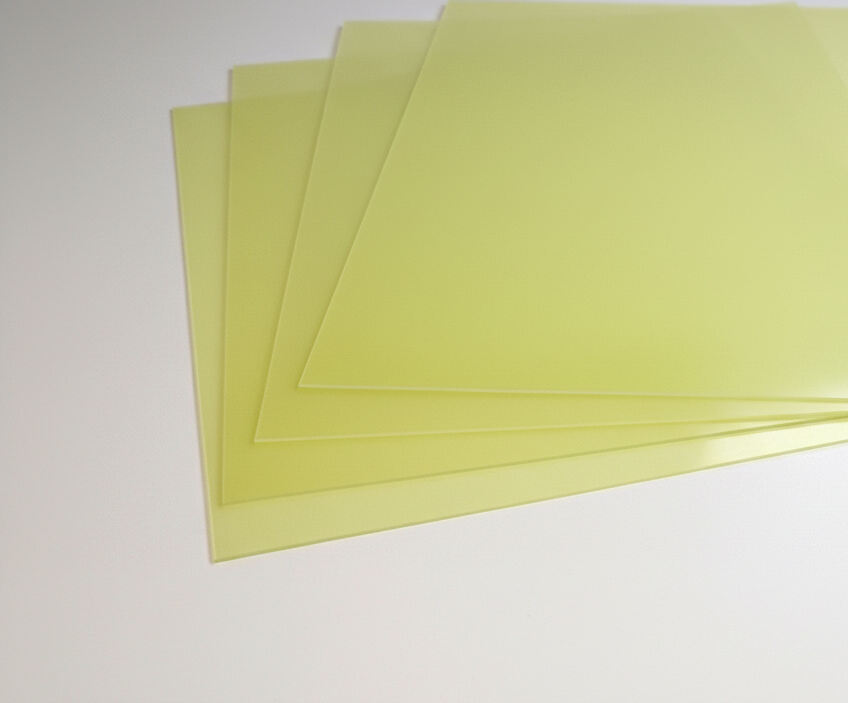
High frequency PCB materials maintain consistent dielectric properties across temperature variations, humidity exposure, and aging cycles that would cause standard PCB substrates to drift beyond acceptable tolerances. This stability stems from advanced resin systems and reinforcement structures engineered specifically for microwave and millimeter-wave applications. Materials like PTFE-based laminates, hydrocarbon ceramics, and specialized polyimide formulations provide dielectric constants ranging from 2.2 to 10.2 with temperature coefficients measured in parts per million rather than percentage points. Communication systems operating in outdoor environments, vehicular applications, or aerospace conditions depend on this material consistency to maintain signal integrity across specification extremes that conventional PCB materials simply cannot accommodate.
The relationship between dielectric constant and signal propagation velocity becomes critical at frequencies above one gigahertz, where wavelengths approach dimensions comparable to PCB trace geometries. A stable dielectric environment ensures predictable impedance matching, controlled phase relationships between differential pairs, and minimal group delay variation across communication channels. When engineers design RF front-ends, antenna feed networks, or phased array systems, dielectric stability translates directly into achievable bandwidth, modulation scheme complexity, and ultimately data throughput capabilities that determine competitive system performance.
Loss Tangent Minimization for Signal Integrity
Signal attenuation through PCB substrate materials increases proportionally with frequency and loss tangent values, making low-loss materials essential for preserving signal strength across transmission paths. High frequency PCB constructions utilize materials with loss tangent values below 0.002 at gigahertz frequencies, compared to 0.020 or higher in standard FR4 substrates. This tenfold reduction in dielectric loss directly translates to extended transmission distances, reduced amplifier requirements, and improved signal-to-noise ratios in communication system architectures. For applications like 5G base stations handling multiple antenna elements or satellite transponders managing weak signals across vast distances, loss tangent becomes a primary material selection criterion.
The economic implications of loss tangent extend beyond material costs to encompass power consumption, thermal management requirements, and overall system complexity. Lower insertion loss through PCB interconnects reduces amplification stages needed to maintain signal levels, decreasing power draw, heat generation, and cooling infrastructure requirements. In battery-powered communication devices, base stations with sustainability mandates, or space applications where every watt matters, the efficiency gains from low-loss PCB materials deliver measurable operational advantages that justify premium material costs through lifecycle economics.
Thermal Expansion Matching for Reliability
High frequency PCB materials exhibit controlled thermal expansion coefficients that match semiconductor packages, metallic housings, and connector systems to prevent mechanical stress accumulation during thermal cycling. This dimensional stability becomes particularly critical when fine-pitch ball grid array packages, high-density interconnects, or precision RF connectors mount to circuit boards experiencing operational temperature swings from negative forty to positive eighty-five degrees Celsius or beyond. Material systems with z-axis expansion coefficients below seventy parts per million per degree Celsius maintain via barrel integrity, prevent pad cracking, and preserve plated through-hole reliability across thousands of thermal cycles.
Communication infrastructure deployed in harsh environments faces thermal stress conditions that accelerate failure mechanisms in poorly matched material systems. High frequency PCB constructions using dimensionally stable materials demonstrate mean time between failure statistics that exceed conventional PCB assemblies by factors of two to five in accelerated life testing. This reliability advantage directly reduces maintenance costs, improves network uptime, and extends equipment replacement cycles in telecommunications infrastructure where service continuity represents both contractual obligations and revenue preservation.
Electrical Design Imperatives for Communication System Performance
Controlled Impedance Architecture Throughout Signal Paths
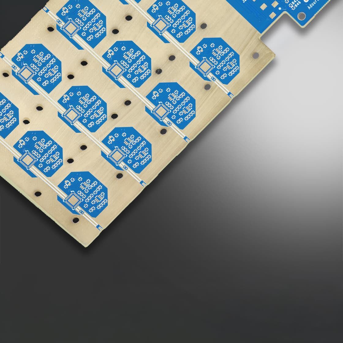
High frequency PCB designs implement precise impedance control across every transmission line segment, ensuring characteristic impedance values match system specifications typically set at fifty ohms for single-ended or one hundred ohms for differential signaling. Achieving impedance tolerances within five to ten percent requires careful calculation of trace widths, dielectric thicknesses, copper weights, and proximity to reference planes throughout the PCB stackup. Advanced communication protocols operating at multi-gigabit data rates cannot tolerate impedance discontinuities that create signal reflections, standing waves, or return loss degradation. Engineers specify controlled impedance PCB fabrication not as a premium option but as baseline requirement for any design handling RF signals or high-speed digital communications.
The manufacturing precision required for controlled impedance achievement distinguishes high frequency PCB production from standard circuit board fabrication. Suppliers must maintain dielectric thickness tolerances within ten percent, control copper plating uniformity to half-ounce variations, and verify impedance through time-domain reflectometry testing of production panels. These process controls add manufacturing complexity and cost but deliver impedance consistency that enables first-pass design success, eliminates field failures from signal integrity issues, and supports product certifications required for communication equipment deployment in regulated markets.
Differential Signaling Implementation for Noise Immunity
Communication systems increasingly adopt differential signaling architectures on high frequency PCB designs to achieve superior common-mode noise rejection and reduced electromagnetic emissions compared to single-ended transmission. Differential pairs maintain tight coupling through matched trace lengths, symmetric routing, and constant spacing that preserves odd-mode impedance throughout signal paths. This design approach becomes essential when communication channels must operate reliably in electrically noisy industrial environments, vehicular applications with ignition interference, or base stations with multiple high-power amplifiers generating electromagnetic fields that could corrupt sensitive receiver circuits.
The PCB layout discipline required for effective differential signaling extends beyond simple trace pairing to encompass via placement, reference plane transitions, and component land pattern design. High frequency PCB fabricators support differential designs through registration accuracy that maintains trace-to-trace spacing tolerances and impedance-controlled processes that balance odd-mode and even-mode impedance relationships. Communication equipment manufacturers specify differential interfaces for everything from serializer-deserializer links to RF balun connections, relying on PCB infrastructure that can preserve the delicate balance and symmetry that differential signaling requires for performance advantage realization.
Ground Plane Strategy for Return Path Management
High frequency PCB stackups incorporate continuous ground planes that provide low-impedance return paths for signal currents, minimize loop areas that generate electromagnetic radiation, and establish stable reference voltages for impedance control. Multi-layer PCB constructions position ground planes adjacent to signal layers, creating microstrip or stripline transmission line structures with predictable electromagnetic behavior across the frequency spectrum. Communication designs handling both RF signals and high-speed digital interfaces often implement separate ground planes for analog and digital circuits, connected at strategic points to prevent noise coupling while maintaining consistent reference potential.
Return path discontinuities created by ground plane splits, via anti-pad clearances, or connector transitions represent primary failure modes in high frequency PCB designs. Current forced to detour around ground plane interruptions creates unintended inductance, generates crosstalk between adjacent circuits, and radiates electromagnetic energy that violates emissions specifications. Expert PCB designers working on communication systems employ specialized simulation tools to visualize return current paths, optimize via placements that stitch ground layers together, and ensure every signal transition maintains clean return path continuity throughout the circuit board architecture.
Manufacturing Process Considerations That Define High Frequency Capability
Copper Surface Roughness Control for Loss Reduction
Signal loss in high frequency PCB conductors increases with surface roughness as skin effect concentrates current flow into a shallow depth where microscopic copper peaks and valleys effectively increase resistive path length. Advanced PCB manufacturing processes specify smooth or very-low-profile copper foils with surface roughness below two micrometers compared to standard electrodeposited copper with roughness exceeding five micrometers. This surface finish selection becomes increasingly critical above five gigahertz where skin depth shrinks to roughly one micrometer, making conductor surface characteristics as important as bulk resistivity for insertion loss performance.
Communication equipment designers balancing cost against performance often specify hybrid PCB constructions using smooth copper on high frequency signal layers while accepting standard copper on power distribution or low-speed control layers. This selective material application optimizes cost structure without compromising critical path performance. PCB manufacturers supporting communication markets invest in specialized copper foil inventory, handle smooth copper carefully to prevent surface damage, and implement lamination processes that preserve surface characteristics through thermal exposure and pressure application required for multilayer construction.
Layer Registration Accuracy for Impedance Consistency
Multilayer high frequency PCB fabrication demands registration accuracy that maintains layer-to-layer alignment within seventy-five to one hundred micrometers to preserve designed impedance relationships throughout the stackup. Misregistration between signal layers and adjacent reference planes changes the dielectric thickness in transmission line cross-sections, shifting impedance away from target values and creating discontinuities at via transitions between layers. Communication system designs with tight impedance tolerances cannot absorb registration variations that standard PCB processes accept, requiring manufacturers to implement optical alignment systems, stabilized substrate materials, and process monitoring that verifies registration throughout production panel populations.
The cost implications of precision registration extend beyond capital equipment to encompass material utilization efficiency, yield rates, and testing requirements that validate layer alignment in finished PCB products. Communication equipment manufacturers qualifying PCB suppliers evaluate registration capability through process audits, cross-sectional analysis, and impedance testing that confirms manufacturing consistency. Suppliers demonstrating superior registration control command price premiums justified by reduced design margins, elimination of impedance tuning components, and field reliability that stems from consistent electrical characteristics matching simulation models used during product development.
Surface Finish Selection for Assembly and Performance
High frequency PCB applications require surface finishes that provide solderability for assembly while minimizing insertion loss through metal-to-metal interfaces in RF signal paths. Finishes like electroless nickel immersion gold, immersion silver, or organic solderability preservative each present tradeoffs between assembly reliability, shelf life, signal performance, and cost. Communication designs with exposed RF connectors, edge-launch interfaces, or press-fit contacts particularly scrutinize surface finish selection as these interfaces directly impact signal transmission without benefit of solder joints that can mitigate finish-related losses.
The interaction between surface finish and high frequency performance manifests through skin effect concentration of current flow in the outermost conductor layers where finish materials reside. Nickel layers, despite excellent corrosion resistance and gold wire bonding compatibility, introduce magnetic loss mechanisms that degrade signal transmission above several gigahertz. Engineers designing communication systems must balance assembly process requirements, environmental exposure protection, and electrical performance implications when specifying PCB surface finishes, often arriving at different conclusions for internal layers protected by solder mask versus exposed contact surfaces requiring mechanical durability.
Application-Specific Benefits Across Communication Technologies
Fifth Generation Wireless Infrastructure Requirements
Fifth generation wireless networks operate across frequency bands from sub-six gigahertz to millimeter wave ranges above twenty-four gigahertz, pushing high frequency PCB requirements into new territory compared to previous mobile generations. Massive MIMO antenna arrays incorporating sixty-four or more elements demand PCB constructions that maintain amplitude and phase matching across dozens of parallel signal paths while managing thermal dissipation from integrated power amplifiers. The combination of high frequencies, dense integration, and power handling creates a demanding environment where PCB material selection, thermal design, and manufacturing precision collectively determine whether base station equipment meets performance specifications.
Communication service providers deploying 5G infrastructure evaluate equipment suppliers partially on the basis of PCB technology sophistication, recognizing that circuit board implementations directly influence coverage range, capacity per sector, and power consumption metrics that drive operational economics. Equipment using optimized high frequency PCB designs achieves measurably better efficiency ratings, reduced cooling requirements, and smaller physical footprints compared to implementations using marginally adequate PCB technology. These advantages translate to lower site acquisition costs, reduced energy expenses, and competitive differentiation in markets where network performance directly correlates with subscriber acquisition and retention.
Satellite Communication Terminal Design
Satellite communication terminals operating in Ku-band, Ka-band, and emerging V-band frequencies require PCB constructions that maintain electrical performance across temperature extremes, operate reliably despite vibration and shock loads, and minimize mass for mobile or airborne applications. High frequency PCB designs using lightweight substrate materials with excellent thermal conductivity address these competing requirements while providing the electrical performance necessary for successful signal transmission across twenty-thousand-mile paths to geostationary satellites or dynamic links to low-earth-orbit constellation networks. The reliability standards for satellite terminals exceed those of terrestrial communication equipment, as field failures in remote locations or mobility platforms result in service disruption costs far exceeding repair expenses.
Terminal manufacturers serving maritime, aviation, military, and emerging automotive satellite connectivity markets specify PCB technologies proven through qualification testing that simulates deployment environment conditions. High frequency PCB suppliers supporting these applications document material properties across temperature ranges, provide thermal cycling test data, and certify manufacturing processes through quality management systems recognized in aerospace and defense sectors. The premium pricing that satellite terminal applications support enables PCB technology selection based primarily on performance and reliability rather than cost minimization, encouraging adoption of most capable materials and processes available in commercial PCB manufacturing.
Automotive Radar and Vehicle-to-Everything Communication
Advanced driver assistance systems and autonomous vehicle sensors rely on millimeter wave radar operating at seventy-seven gigahertz alongside vehicle-to-everything communication protocols using 5.9 gigahertz spectrum allocations. These automotive applications impose unique challenges combining high frequency PCB requirements with automotive qualification standards, extreme temperature cycling, vibration resistance, and cost structures aligned with consumer vehicle economics rather than aerospace budgets. Circuit board technologies meeting these requirements enable safety-critical functions like collision avoidance, adaptive cruise control, and intersection coordination that define next-generation vehicle capabilities.
Automotive electronics manufacturers transitioning from conventional PCB constructions to high frequency capable designs for radar and V2X applications invest significantly in supply chain development, testing infrastructure, and design methodology evolution. The volume potential of automotive markets justifies this investment while driving cost reduction in high frequency PCB manufacturing through economies of scale previously unavailable when production concentrated in aerospace and telecommunications infrastructure. Communication system designers benefit from automotive market expansion as improved material availability, manufacturing capacity growth, and process maturity make high frequency PCB technology increasingly accessible across diverse application domains.
Economic Justification and Total Cost of Ownership Analysis
Performance Advantage Monetization in Competitive Markets
Communication equipment manufacturers utilizing optimal high frequency PCB implementations achieve measurable performance advantages including extended range, increased throughput, reduced latency, and improved reliability compared to products using marginal PCB technology. These technical superiorities translate into competitive differentiation that supports premium pricing, wins design selections in competitive procurements, and builds brand reputation that influences future purchase decisions. The incremental cost of superior PCB technology typically represents less than five percent of finished communication equipment value while enabling performance distinctions that justify ten to twenty percent price premiums in B2B equipment sales.
Market analysis of communication equipment categories consistently demonstrates correlation between PCB technology sophistication and market share leadership, particularly in performance-sensitive segments like infrastructure equipment, test instrumentation, and defense electronics. Companies committed to PCB technology investment as strategic differentiator rather than cost minimization opportunity build sustainable competitive advantages difficult for followers to replicate without similar multiyear development commitments. This dynamic makes high frequency PCB selection decisions strategic choices with implications extending beyond individual product programs to encompass corporate positioning and long-term market presence.
Lifecycle Cost Implications Beyond Initial Procurement
Total cost of ownership analysis for communication systems reveals that PCB-related costs extend far beyond initial circuit board procurement to encompass assembly yield rates, field failure rates, warranty expenses, and product obsolescence timing. High frequency PCB designs using appropriate materials and manufacturing processes demonstrate assembly yields exceeding ninety-eight percent compared to eighty to ninety percent yields common when marginal PCB technologies attempt to meet demanding specifications. This yield differential alone often justifies PCB cost premiums through reduced rework expenses, shorter production cycles, and improved on-time delivery performance.
Field reliability data accumulated across communication equipment lifecycles shows PCB-related failure modes including via barrel cracking, pad delamination, and dielectric breakdown account for fifteen to thirty percent of all product returns depending on application environment severity. Equipment using properly specified high frequency PCB constructions experiences failure rates one-third to one-fifth those of products using inadequate PCB technology, directly reducing warranty costs, service infrastructure requirements, and customer satisfaction issues that damage brand value. These lifecycle benefits compound over product generations as companies build reliability reputations that influence customer loyalty and competitive positioning in markets where equipment downtime carries significant operational consequences.
Design Reuse and Platform Scalability Benefits
Communication equipment platforms built on robust high frequency PCB foundations support design reuse across product families, frequency band variants, and power level options that would require complete redesign if built on marginal PCB technology operating near performance limits. This scalability advantage reduces non-recurring engineering costs, accelerates derivative product development, and enables rapid response to market opportunities or customer-specific requirements. The value of design reuse particularly manifests in markets with short technology lifecycles where time-to-market advantages determine competitive success and late market entries face significant disadvantage regardless of technical merit.
Companies establishing high frequency PCB design methodologies, supplier relationships, and internal expertise create organizational capabilities that benefit subsequent product generations and parallel development programs. This knowledge accumulation represents intangible asset value exceeding the sum of individual product development investments, establishing barriers to entry that protect market position against competitors lacking equivalent organizational competency. Strategic PCB technology decisions thus carry implications extending throughout product portfolios and across multiyear planning horizons that justify investment levels inconsistent with narrow project-specific cost optimization but entirely rational from enterprise perspective.
FAQ
What frequency range defines high frequency PCB applications?
High frequency PCB classifications typically begin around five hundred megahertz where conventional FR4 materials start exhibiting measurable signal loss and dielectric property variations that impact circuit performance. Practical applications span from this threshold through millimeter wave frequencies exceeding one hundred gigahertz, with most commercial communication systems operating between one and forty gigahertz. The specific frequency at which designers transition from standard to high frequency PCB materials depends on performance requirements, loss budgets, and cost constraints particular to each application rather than absolute frequency thresholds.
How does high frequency PCB cost compare to standard circuit boards?
High frequency PCB material costs typically range from three to ten times standard FR4 pricing depending on specific material selection, with PTFE-based laminates at the premium end and hydrocarbon ceramics offering mid-range options. Manufacturing costs add premiums of thirty to one hundred percent due to specialized processes, tighter tolerances, and additional testing requirements. For complete communication system assemblies, PCB costs typically represent five to fifteen percent of total product cost, making performance advantages and reliability benefits economically justifiable despite absolute cost premiums compared to conventional circuit board technology.
Can existing PCB designs be converted to high frequency materials?
Direct material substitution rarely succeeds because high frequency PCB materials exhibit different dielectric constants, thermal expansion properties, and processing requirements compared to standard substrates. Successful conversions require impedance recalculation, potential trace width adjustments, via structure modifications, and assembly process revisions to accommodate material property differences. Most communication equipment transitions to high frequency PCB technology occur during major product redesigns when engineering resources support comprehensive design optimization rather than attempting minimal-change material substitutions that risk introducing new failure mechanisms while inadequately capturing performance benefits.
What testing validates high frequency PCB performance?
High frequency PCB validation combines time-domain reflectometry for impedance verification, vector network analyzer measurements for insertion loss and return loss characterization, and environmental stress testing including thermal cycling, humidity exposure, and vibration qualification. Communication equipment manufacturers typically require PCB suppliers to provide material property documentation, process capability statistics, and sample testing results before production authorization. Ongoing quality monitoring employs impedance coupon testing on production panels, microsection analysis verifying layer registration and copper quality, plus electrical testing of finished PCB assemblies confirming performance consistency across manufacturing lots.
Table of Contents
- Material Science Foundations That Enable High Frequency Performance
- Electrical Design Imperatives for Communication System Performance
- Manufacturing Process Considerations That Define High Frequency Capability
- Application-Specific Benefits Across Communication Technologies
- Economic Justification and Total Cost of Ownership Analysis
- FAQ