
 EN
EN
A PCB pad is one of the most fundamental elements in printed circuit board design. Every component mounted on a board relies on a PCB pad to form a stable electrical and mechanical connection. Without a properly designed PCB pad, solder joints fail, signals degrade, and components may detach under thermal or mechanical stress. Understanding what a PCB pad is and how it functions is essential knowledge for any engineer, designer, or procurement professional working in electronics manufacturing.
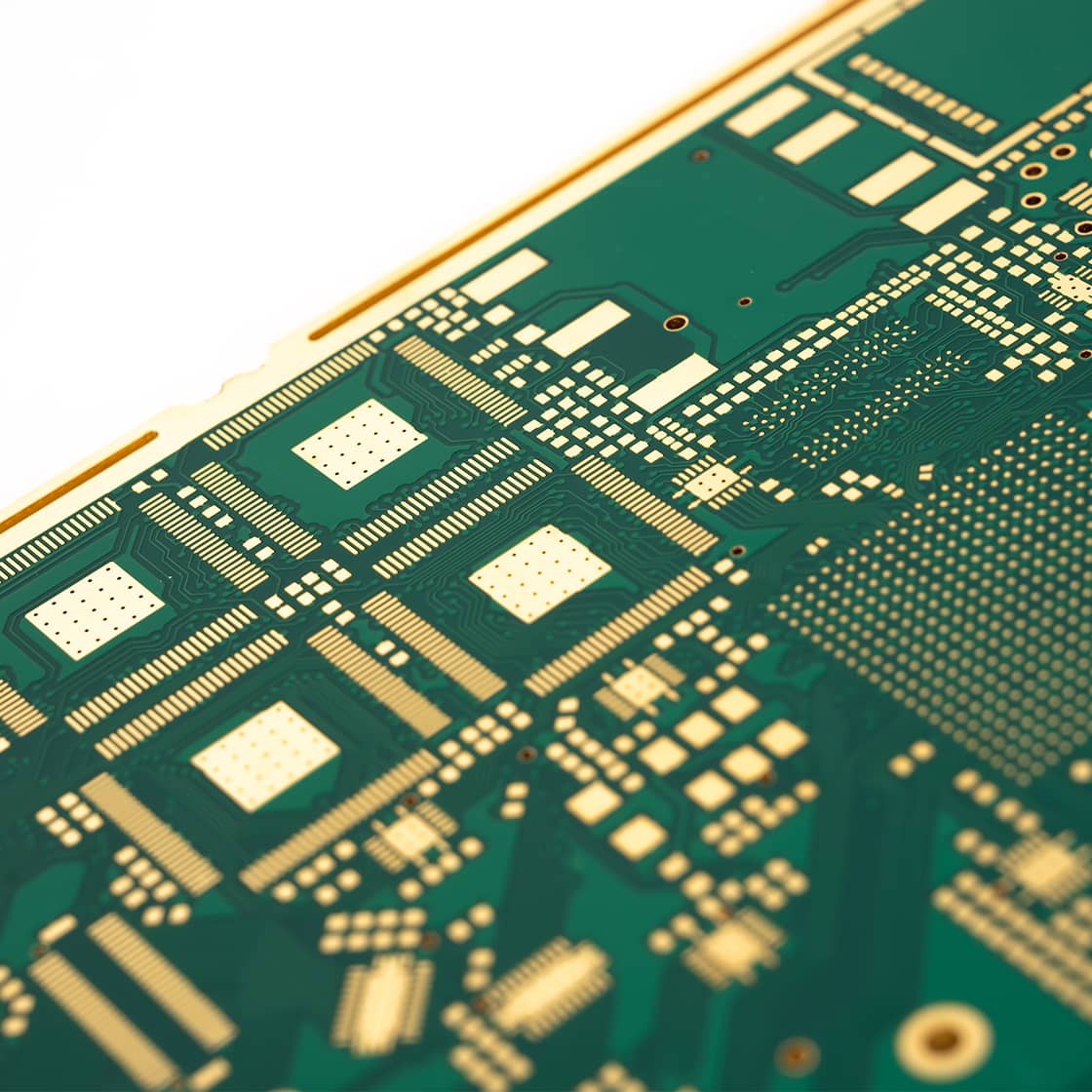
A PCB pad is a small exposed area of copper on the surface of a printed circuit board where a component lead or terminal is soldered. Each PCB pad acts as a landing zone for solder, anchoring the component in place and creating a conductive pathway into the board's circuitry. The geometry, material, finish, and placement of a PCB pad are all carefully engineered to match the component's footprint and the assembly process being used. This guide covers everything you should know about PCB pads, from their basic definition to their types, design considerations, and common applications.
The Core Definition and Function of a PCB Pad
What a PCB Pad Actually Does
At its most basic level, a PCB pad serves two purposes: it provides a solderable surface for attaching a component, and it connects that component electrically to the rest of the circuit. The PCB pad is the interface between the physical component and the conductive traces routed through the board. When solder is applied during assembly, it flows onto the PCB pad, wets the copper surface, and bonds the component terminal to the board. This joint must be mechanically strong enough to survive vibration, thermal cycling, and handling while remaining electrically continuous throughout the product's lifespan.
Each PCB pad is defined in the board's design files using a footprint library. The footprint specifies the exact dimensions, shape, and spacing of every PCB pad associated with a particular component. Getting these dimensions right is critical because an undersized PCB pad may not retain solder reliably, while an oversized PCB pad can cause bridging between adjacent connections. Designers must match the PCB pad geometry to the component datasheet and the assembly process tolerances to ensure yield and reliability.
The Role of Copper and Surface Finish on a PCB Pad
The base material of any PCB pad is copper, typically 1 oz or 2 oz per square foot in thickness. Raw copper oxidizes quickly, which degrades solderability. For this reason, every PCB pad receives a surface finish treatment during fabrication. Common surface finishes applied to a PCB pad include HASL (Hot Air Solder Leveling), ENIG (Electroless Nickel Immersion Gold), OSP (Organic Solderability Preservative), and ENEPIG. Each finish affects the shelf life, solderability, planarity, and cost of the PCB pad. ENIG is widely preferred for fine-pitch PCB pad layouts because it offers a flat, reliable surface that supports accurate component placement.
Types of PCB Pads and Their Design Variations
SMD Pads Versus Through-Hole Pads
The two primary categories of PCB pad are surface-mount device (SMD) pads and through-hole pads. An SMD PCB pad is a flat copper area on the board surface with no drilled hole. Components with flat terminals, such as resistors, capacitors, and ICs in QFP or QFN packages, are mounted directly onto these pads. SMD PCB pad designs are preferred in modern high-density assemblies because they allow components on both sides of the board and support automated pick-and-place processes efficiently.
A through-hole PCB pad includes a drilled hole through the board, surrounded by a copper annular ring. The component lead is inserted through the hole and soldered on the opposite side. Through-hole PCB pads provide excellent mechanical strength, making them suitable for connectors, power terminals, and components subject to physical stress. The annular ring of a through-hole PCB pad must meet minimum width requirements to maintain reliable conductivity after drilling tolerances are applied during fabrication.
Specialized PCB Pad Formats
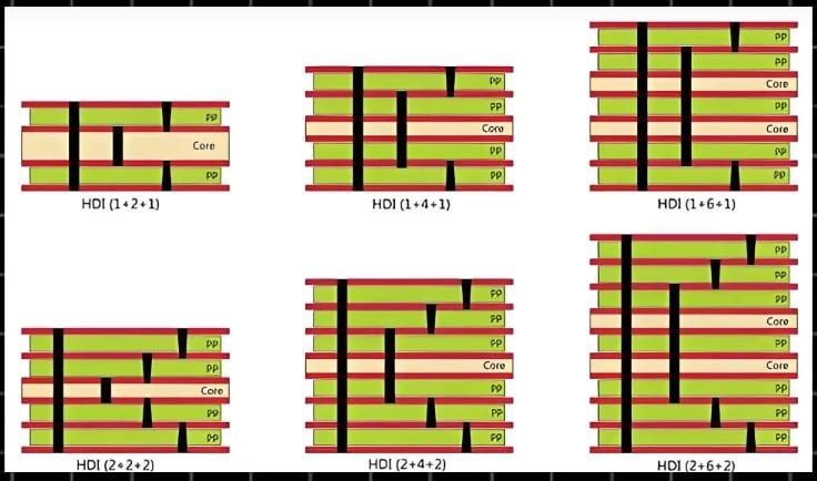
Beyond standard SMD and through-hole formats, there are several specialized PCB pad types used in advanced board designs. A via-in-pad is a PCB pad that incorporates a filled or plated via directly within the pad area, enabling high-density routing beneath components such as BGA packages. This PCB pad format is common in compact devices where routing space is extremely limited. Thermal pads are another important variation, typically found under power management ICs and used to conduct heat away from the component into the board's copper planes. A test pad is a dedicated PCB pad placed at strategic locations to allow in-circuit testing probes to contact the board without disturbing assembly.
PCB Pad Design Considerations for Reliable Assembly
Pad Size, Shape, and Spacing Rules
Designing a PCB pad correctly requires attention to size, shape, and spacing. The size of a PCB pad must provide enough area for solder to form a strong fillet around the component terminal. Industry guidelines and IPC standards define minimum and optimal PCB pad dimensions for each component type and package. Rounded PCB pad corners are often preferred for SMD pads because they reduce solder stress concentration points. Spacing between adjacent PCB pads must account for solder mask tolerances and paste stencil apertures to prevent bridging during reflow soldering.
The solder mask opening around a PCB pad is equally important. A solder mask defined (SMD) PCB pad has its opening smaller than the copper area, giving the mask material overlap onto the pad edges. A non-solder-mask-defined (NSMD) PCB pad has a mask opening larger than the copper, leaving the entire PCB pad exposed. NSMD configurations are generally preferred for fine-pitch components because they provide more consistent solder joint geometry. The choice between SMD and NSMD for each PCB pad type should align with the component package specifications and fabrication capabilities.
Thermal Relief and Copper Pour Connections
When a PCB pad connects to a large copper plane, thermal relief spokes are typically added. Without thermal relief, heat dissipates too rapidly into the copper pour during soldering, preventing the PCB pad from reaching the temperature needed for a proper solder joint. Thermal relief patterns connect the PCB pad to the copper plane through narrow spoke sections, slowing heat transfer enough to allow consistent soldering. For high-current applications, however, solid connections between the PCB pad and copper planes may be preferred to minimize resistance, requiring higher soldering temperatures to compensate.
FAQ
What is the difference between a PCB pad and a via?
A PCB pad is a copper area on the board surface used for soldering a component. A via is a drilled and plated hole used to carry signals between layers of the board. A via-in-pad combines both by placing a via directly inside a PCB pad, which is useful in high-density layouts where routing space beneath components is needed.
Why does PCB pad size matter for assembly quality?
PCB pad size directly affects solder joint quality. A PCB pad that is too small may not hold enough solder to form a reliable joint, leading to cold or weak connections. A PCB pad that is too large can cause solder to spread unevenly or bridge between adjacent pads. Correct PCB pad sizing, based on the component footprint and IPC standards, is critical for high assembly yield.
What surface finish is best for a PCB pad?
The best surface finish for a PCB pad depends on the application. ENIG is widely favored for fine-pitch PCB pad designs because of its flat surface and strong solderability. HASL is cost-effective for standard through-hole PCB pad applications. OSP offers good solderability with a lower environmental footprint. Choosing the right finish for each PCB pad type should consider shelf life requirements, assembly process, and budget constraints.