
 EN
EN
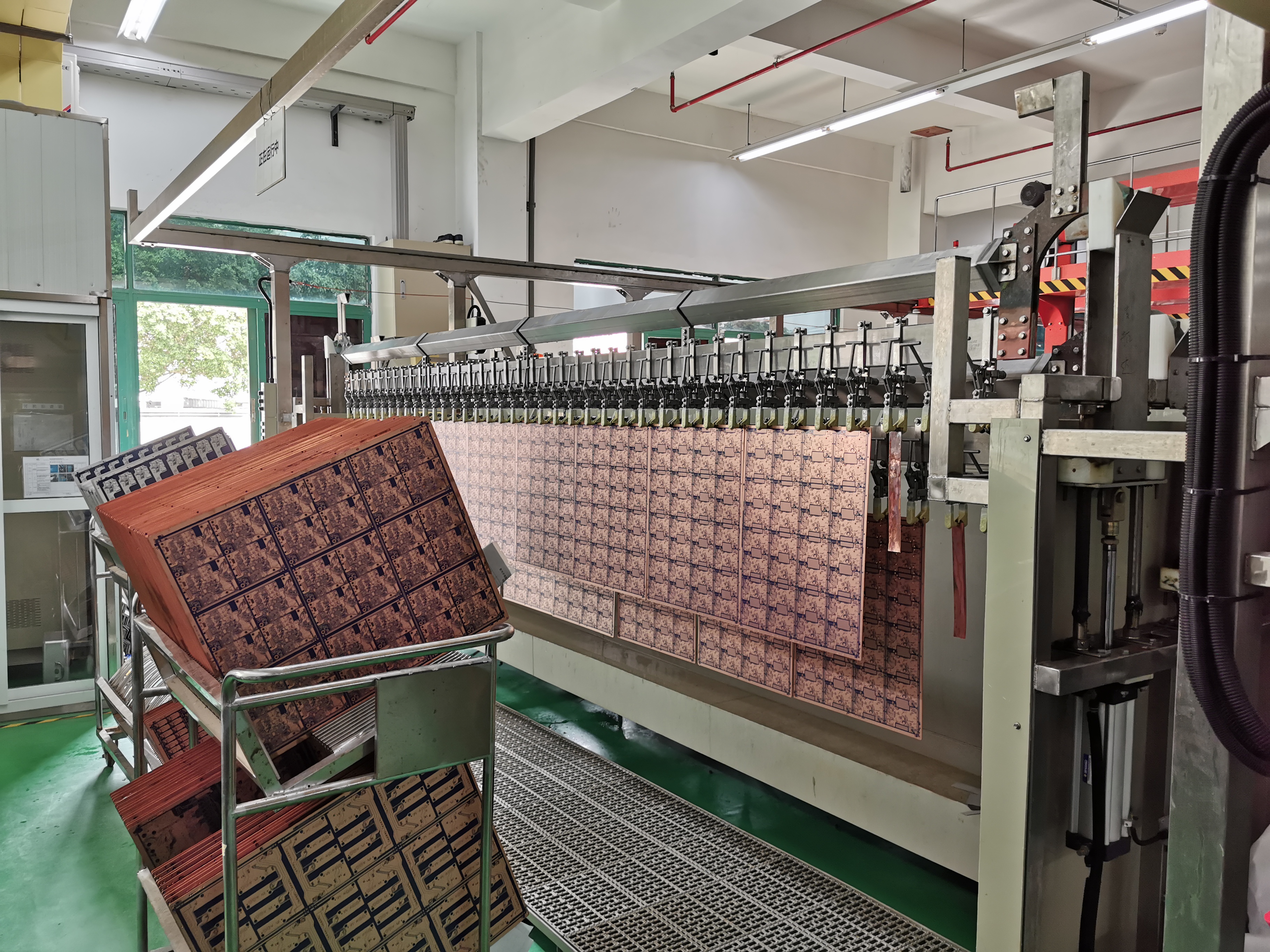
Building a custom mechanical keyboard starts with one foundational component: the PCB. A PCB, or printed circuit board, is the electronic backbone of every keyboard. It registers each keypress and transmits that signal to your computer. Without a well-designed PCB, even the finest switches and keycaps will underperform. Understanding how the PCB works and how to choose the right one is the critical first step in any serious keyboard build project.

A custom keyboard PCB differs significantly from the generic PCB found in mass-market keyboards. Custom PCB options allow builders to select specific layouts, switch mounting styles, and firmware support. Whether you are assembling a 65%, a tenkeyless, or a full-size board, the PCB you choose defines what is possible in your build. Every decision downstream — from the case to the stabilizers — depends on the PCB dimensions and feature set you commit to early in the process.
Understanding PCB Types for Keyboard Builds
Hot-Swap vs. Soldered PCB Designs
One of the first decisions a keyboard builder faces is choosing between a hot-swap PCB and a soldered PCB. A hot-swap PCB uses pre-installed sockets that allow switches to be inserted and removed without any soldering. This makes the hot-swap PCB ideal for builders who want flexibility to swap switches frequently. A soldered PCB requires switches to be permanently attached using a soldering iron, which provides a more secure and often more electrically stable connection. For builders who have settled on a specific switch type, a soldered PCB can deliver slightly lower latency and firmer switch seating.
Both PCB types are widely used in the custom keyboard community. The hot-swap PCB is generally recommended for beginners, as it lowers the barrier to experimentation. The soldered PCB, by contrast, rewards builders with more advanced skills and a clear vision for their final configuration. Knowing which PCB type fits your workflow will save time, cost, and frustration throughout the build.
PCB Layouts and Size Compatibility
Every PCB is designed around a specific keyboard layout. Common PCB sizes include 40%, 60%, 65%, 75%, tenkeyless (TKL), and full-size formats. Each PCB layout corresponds to a defined set of key positions and dimensions. Choosing a PCB that does not match your case or plate will result in mounting failures. Always verify that the PCB layout aligns precisely with the keyboard case you have selected before purchasing or ordering a custom PCB.
Some PCB designs offer multi-layout support, meaning a single PCB can accommodate different keycap configurations through multiple switch footprints. This type of PCB gives builders more flexibility when choosing keycap sets or experimenting with alternative layouts such as split spacebars or stepped modifiers. Multi-layout PCB designs are especially popular in the enthusiast community for their versatility.
How a PCB Is Built and What Makes It Custom
PCB Layer Structure and Material Choices
A keyboard PCB is typically a two-layer or four-layer board made from FR4 fiberglass substrate. The PCB layers carry copper traces that connect each switch position to the microcontroller. The microcontroller on the PCB reads the switch matrix and translates physical keypresses into digital signals. For most keyboard builds, a two-layer PCB provides sufficient routing capacity. High-feature PCB designs with RGB lighting, per-key LEDs, or complex macro systems may benefit from a four-layer PCB to manage signal integrity.
PCB thickness also affects the typing feel of the finished keyboard. A standard PCB thickness of 1.6mm is the most common choice and fits the majority of keyboard cases. Thinner PCB options, such as 1.2mm, can flex slightly under typing force, which some builders find produces a softer sound profile. The right PCB thickness depends on the acoustic and tactile goals you have defined for the build.
Firmware and PCB Programmability
A custom PCB gains much of its value from firmware support. QMK and VIA are the two most widely used open-source firmware platforms for keyboard PCB designs. A PCB flashed with QMK firmware allows builders to remap every key, create macro layers, adjust RGB settings, and configure tap-hold behaviors — all without proprietary software. VIA adds a real-time graphical interface that makes PCB remapping accessible without compiling code.
When evaluating a PCB for your build, confirm that it supports QMK or VIA before committing. A PCB with limited or no firmware programmability significantly restricts the customization potential of the entire keyboard. Firmware compatibility is one of the most important PCB specifications to verify during the selection process.
Step-by-Step Guide to Building with a Keyboard PCB
Preparing the PCB Before Assembly
Before installing any switches, the PCB should be tested using a switch tester tool or by shorting each switch socket with metal tweezers while monitoring keypress output in a keyboard testing application. This PCB testing step identifies any dead sockets or faulty solder joints on the PCB before assembly, saving significant time during troubleshooting. Mark any problematic positions on the PCB with tape so they can be addressed before soldering or switch insertion begins.
If your PCB supports per-key RGB LEDs, install the LED components before soldering switches, as the LEDs sit beneath the switches on most PCB designs. Lubing stabilizers and mounting them on the PCB before switch installation is also standard practice. Stabilizers attach directly to the PCB through either a screw-in or clip-in mounting system. Screw-in stabilizers provide better retention and are preferred for high-quality PCB builds.
Soldering Switches and Final PCB Assembly
For a soldered PCB, install switches into the plate first, then align the plate-switch assembly onto the PCB. Ensure each switch pin is properly inserted through the PCB footprint before soldering. Apply heat to each pin for no more than three seconds and feed solder until a clean joint forms. A properly soldered PCB joint is shiny and smooth. Cold or dull solder joints on the PCB must be reflowed to avoid intermittent keypress failures.
Once all switches are soldered, test the PCB again through the full switch matrix before closing the case. This final PCB test confirms that every key registers correctly and that no bridges or cold joints exist. After the PCB passes testing, mount the assembly into the keyboard case using the designated PCB mounting points. Tighten all screws evenly to prevent the PCB from flexing unevenly inside the case.
FAQ
What is the difference between a PCB and a keyboard plate?
A PCB is the electronic circuit board that registers keypresses and transmits signals. A plate is a structural layer that sits above the PCB and holds the switches in alignment. The plate does not carry any electrical signals; its role is mechanical. Both the PCB and the plate are necessary for a fully assembled keyboard, and their compatibility must be confirmed before purchasing either component.
Can I design a completely custom PCB for my keyboard?
Yes, fully custom PCB design is possible using EDA software such as KiCad. A custom PCB allows you to specify an exact layout, include specific microcontrollers, and integrate features not available on off-the-shelf PCB options. Custom PCB fabrication is handled by PCB manufacturers who produce the board to your Gerber file specifications. This route requires technical knowledge but gives builders complete control over every PCB attribute.
How do I know if a PCB is compatible with my keyboard case?
PCB compatibility with a case depends on the PCB layout size, mounting hole positions, and USB port placement. Always compare the PCB dimensions and mounting pattern against the case documentation before ordering. Many keyboard cases list compatible PCB models in their specifications. When building a fully custom keyboard, sourcing the case and PCB from the same design ecosystem ensures proper alignment and reduces the risk of fitment issues during final assembly.