
Understanding the Essential Components of Modern Printed Circuit Boards
Printed circuit boards (PCBs) are the foundation of modern electronics, serving as the platform that connects and supports various electronic components. These intricate boards are crafted from multiple materials and layers, each serving a specific purpose in ensuring reliable electronic device operation. From smartphones to industrial equipment, PCB materials play a crucial role in determining the performance, durability, and reliability of electronic devices.
The composition of PCBs has evolved significantly since their inception, with manufacturers now employing advanced materials and sophisticated manufacturing processes to meet the growing demands of modern electronics. Understanding these materials and their properties is essential for engineers, manufacturers, and anyone involved in electronic product development.
Core Materials and Substrate Composition
Base Material Selection and Properties
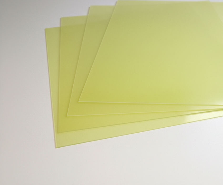
The foundation of any PCB begins with its base material, typically composed of a glass-reinforced epoxy laminate known as FR-4. This composite material combines woven fiberglass cloth with an epoxy resin binder, creating a strong, heat-resistant, and electrically insulating substrate. FR-4 has become the industry standard due to its excellent balance of electrical, mechanical, and thermal properties.
Alternative base materials include FR-2 (phenolic cotton paper), aluminum, ceramic, and polyimide. Each material offers unique characteristics suited for specific applications. For instance, polyimide boards excel in high-temperature environments, while ceramic substrates provide superior thermal management for power electronics.
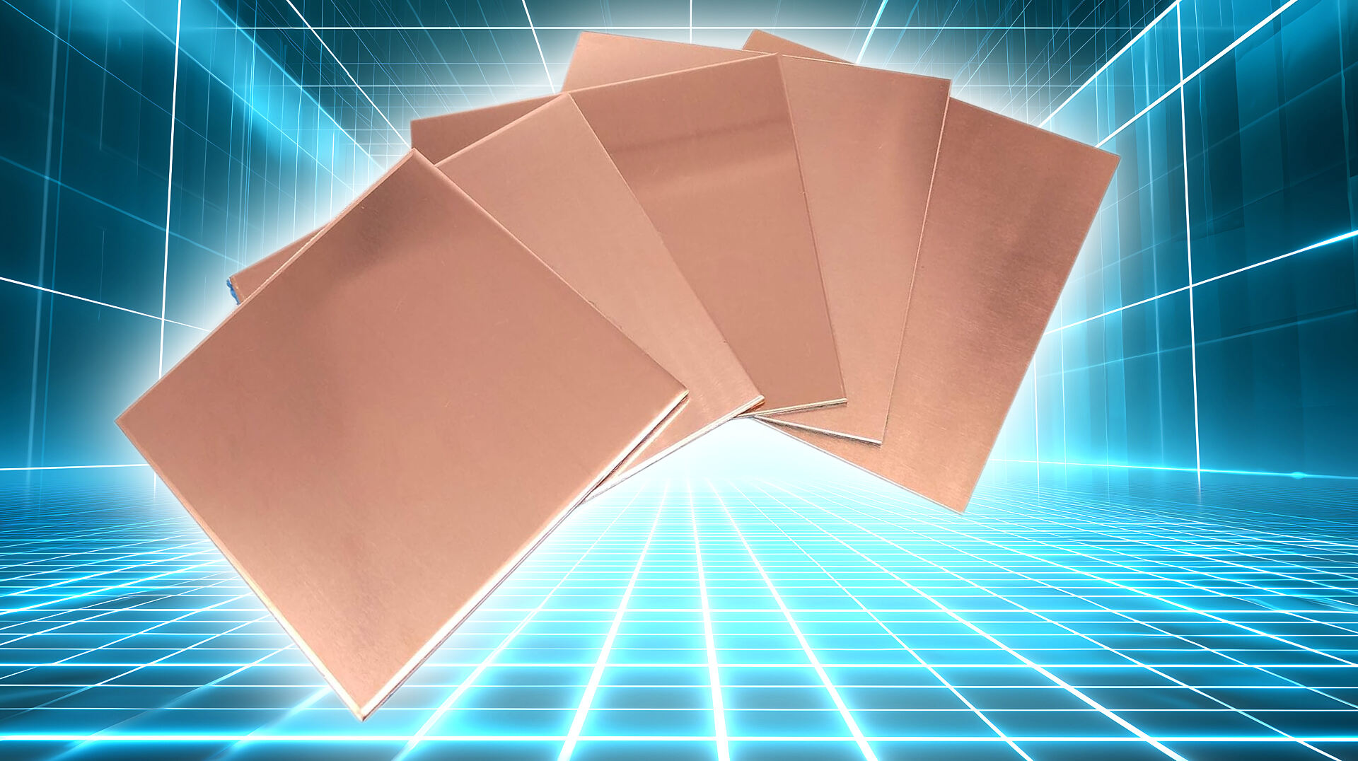
Copper Foil and Conductivity Layers
Copper foil serves as the primary conductive material in PCBs, typically available in varying weights measured in ounces per square foot. The standard thickness is 1-ounce copper, though heavier weights are used for high-current applications. The copper layer is bonded to the substrate through a combination of heat and pressure during manufacturing.
The quality and thickness of copper foil significantly impact the board's electrical performance. Manufacturers must carefully consider factors such as current-carrying capacity, impedance control, and signal integrity when selecting copper specifications.
Specialized Layers and Their Functions
Solder Mask and Surface Protection
The solder mask layer is a thin, polymer-based coating applied to the copper traces, protecting them from oxidation and preventing solder bridges during component assembly. This layer gives PCBs their characteristic green color, though other colors are available for specific applications or branding purposes.
Modern solder masks incorporate advanced materials that provide enhanced protection against environmental factors, improved adhesion, and better compatibility with lead-free soldering processes. The quality of the solder mask significantly influences the board's long-term reliability and manufacturing yield.
Silkscreen and Component Markings
The silkscreen layer, typically white in color, provides essential information such as component designators, polarity indicators, and manufacturer markings. This layer uses specialized inks that adhere well to the solder mask and maintain legibility throughout the board's lifetime.
Advanced silkscreen technologies now allow for higher resolution printing, enabling more detailed markings on increasingly compact boards. This improvement supports the trend toward miniaturization in electronic devices while maintaining assembly accuracy.
Advanced Manufacturing Considerations
Multi-layer Construction Techniques
Modern PCBs often incorporate multiple layers, with some complex designs featuring 20 or more layers. These layers are bonded together using prepreg material, which consists of partially cured epoxy-impregnated fiberglass. The layering process requires precise control of temperature, pressure, and timing to ensure proper bonding and prevent delamination.
The arrangement of power, ground, and signal layers within a multi-layer PCB requires careful planning to optimize electrical performance while maintaining manufacturability. Engineers must consider factors such as impedance control, crosstalk reduction, and thermal management when designing layer stackups.
Surface Finish Options
Surface finishes protect exposed copper pads and facilitate component soldering. Common options include HASL (Hot Air Solder Leveling), ENIG (Electroless Nickel Immersion Gold), OSP (Organic Solderability Preservative), and immersion tin or silver. Each finish offers distinct advantages in terms of shelf life, solderability, and cost.
The selection of surface finish impacts both the manufacturing process and the long-term reliability of the assembled board. Considerations include component compatibility, environmental regulations, and specific application requirements.
Environmental and Regulatory Considerations
Material Compliance Standards
PCB materials must comply with various environmental regulations, including RoHS (Restriction of Hazardous Substances) and REACH (Registration, Evaluation, Authorization and Restriction of Chemicals). These standards influence material selection and manufacturing processes, particularly regarding lead-free requirements and flame retardant compositions.
Manufacturers must maintain detailed documentation of material compliance and regularly update their processes to meet evolving environmental standards. This commitment to environmental responsibility has driven innovation in PCB materials and processing techniques.
Sustainability and Recycling
The electronics industry is increasingly focusing on sustainable practices, including the development of eco-friendly PCB materials and recycling processes. New biodegradable substrates and recyclable composites are being researched to reduce environmental impact while maintaining performance standards.
End-of-life considerations now play a crucial role in material selection and design decisions. Manufacturers are developing processes to recover valuable materials from PCBs while minimizing environmental hazards associated with electronic waste.
Frequently Asked Questions
What determines the choice of PCB base material?
The selection of PCB base material depends on several factors including operating temperature requirements, mechanical stress tolerance, electrical properties, and cost considerations. FR-4 is the most common choice for general applications, while specialized materials like polyimide or ceramic are chosen for high-performance or extreme environment applications.
How do different copper weights affect PCB performance?
Copper weight affects current-carrying capacity, heat dissipation, and impedance characteristics. Heavier copper weights (2 oz or more) are typically used for high-current applications or when better heat distribution is needed, while lighter weights (0.5 or 1 oz) are standard for signal layers and general-purpose applications.
What role does the solder mask play in PCB protection?
The solder mask serves multiple functions: it prevents oxidation of copper traces, provides electrical insulation between conductors, prevents solder bridges during assembly, and protects the board from environmental factors such as moisture and dust. The quality and type of solder mask significantly impact the board's reliability and manufacturing yield.