
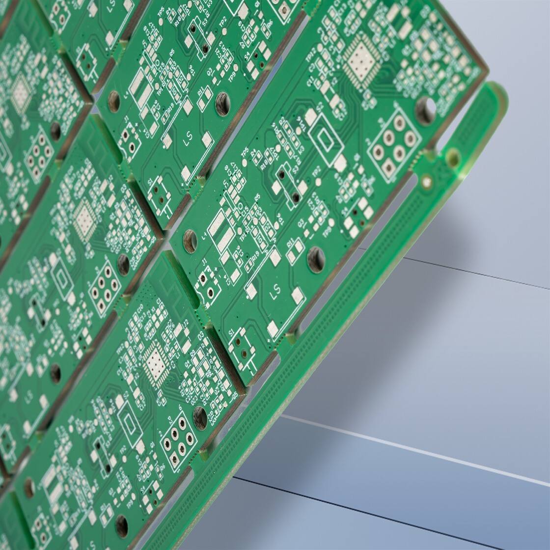
In the evolving landscape of electronics manufacturing, the push toward environmentally responsible materials has led to significant innovations in printed circuit board technology. A halogen free PCB represents a critical advancement in this direction, designed to eliminate hazardous halogenated compounds from the substrate materials used in circuit board fabrication. These specialized boards address growing environmental regulations and health concerns associated with traditional PCB materials that contain bromine and chlorine-based flame retardants. Understanding what constitutes a halogen free PCB requires examining both the material science behind these boards and the regulatory frameworks driving their adoption across global electronics markets.
The fundamental distinction of halogen free PCB construction lies in the deliberate exclusion of halogen elements—specifically bromine and chlorine—from the laminate materials and solder mask compositions. Traditional circuit boards have historically relied on brominated and chlorinated flame retardants to meet fire safety standards, but these compounds release toxic dioxins and furans when burned or disposed of improperly. The halogen free alternative employs phosphorus-based or nitrogen-based flame retardants that provide equivalent fire resistance without the environmental toxicity. This material substitution represents more than a simple ingredient swap; it requires comprehensive re-engineering of the PCB substrate chemistry to maintain electrical performance, thermal stability, and manufacturing compatibility while meeting stringent environmental compliance standards established by directives such as RoHS and WEEE.
Material Composition and Chemical Standards
Defining Halogen Content Thresholds
The classification of a halogen free PCB follows specific quantitative criteria established by industry standards organizations. According to IPC-4101 specifications and IEC 61249-2-21 standards, a circuit board qualifies as halogen free when chlorine content remains below 900 parts per million and bromine content stays under 900 ppm, with total combined halogen content not exceeding 1500 ppm. These precise thresholds distinguish genuinely halogen free boards from low-halogen alternatives that may still contain problematic compounds above trace levels. The measurement protocols involve sophisticated analytical techniques including ion chromatography and X-ray fluorescence spectroscopy to verify compliance. Manufacturers must test both the base laminate materials and the final assembled PCB to ensure all layers and components meet these stringent requirements throughout the production process.
Alternative Flame Retardant Systems
Replacing halogenated flame retardants in PCB manufacturing requires carefully engineered alternative compounds that maintain fire safety performance without environmental hazards. Phosphorus-based flame retardants function through a char-forming mechanism that creates an insulating layer during combustion, effectively starving the fire of oxygen and fuel. Nitrogen-containing compounds such as melamine derivatives work synergistically with phosphorus systems to enhance flame suppression. Metal hydroxides including aluminum trihydroxide and magnesium hydroxide release water vapor when heated, diluting flammable gases and cooling the combustion zone. The selection of appropriate flame retardant systems depends on the specific resin chemistry, target glass transition temperature, and electrical performance requirements of the PCB application. Modern halogen free formulations achieve UL 94 V-0 flammability ratings—the highest fire safety classification—while maintaining the dielectric properties essential for high-frequency signal transmission and power integrity.
Resin Matrix Technologies
The resin systems used in halogen free PCB laminates represent advanced polymer chemistry designed to work effectively with non-halogenated flame retardants. Epoxy resins modified with phosphorus-containing reactive groups provide inherent flame resistance at the molecular level rather than relying solely on additive flame retardants. Polyphenylene oxide blends combined with epoxy create hybrid resin systems with excellent thermal stability and low moisture absorption characteristics. Cyanate ester resins offer superior high-frequency electrical properties for demanding RF and microwave applications where signal loss must be minimized. The glass transition temperature of halogen free laminates typically ranges from 150°C to 180°C, comparable to or exceeding conventional FR-4 materials. Resin formulation must balance multiple performance parameters including coefficient of thermal expansion, peel strength for copper adhesion, chemical resistance to processing fluids, and long-term reliability under thermal cycling conditions that PCB assemblies experience throughout their operational lifespan.
Environmental and Regulatory Drivers
Global Compliance Mandates
The adoption of halogen free PCB technology stems directly from increasingly stringent environmental regulations governing electronics manufacturing and waste management. The European Union's Restriction of Hazardous Substances directive establishes the regulatory foundation by limiting specific toxic materials in electrical equipment sold within member states. While RoHS primarily targets heavy metals and certain brominated flame retardants in the original directive, subsequent amendments and national implementations have expanded scrutiny of halogenated compounds more broadly. The Waste Electrical and Electronic Equipment directive complements RoHS by addressing end-of-life disposal and recycling requirements, creating economic incentives for manufacturers to design products that minimize toxic emissions during waste incineration. Japan's Green Procurement guidelines and China's Management Methods for Controlling Pollution by Electronic Information Products establish parallel regulatory frameworks in Asian markets. These overlapping jurisdictions create practical business imperatives for electronics manufacturers to standardize on halogen free PCB materials across their global product portfolios rather than maintaining region-specific material specifications.
Corporate Environmental Commitments
Beyond regulatory compliance, major electronics brands have established voluntary environmental policies that mandate halogen free materials throughout their supply chains. Leading computer manufacturers, telecommunications equipment providers, and consumer electronics companies publicly commit to eliminating halogenated flame retardants as part of broader corporate sustainability initiatives. These commitments cascade through the electronics supply chain, requiring PCB fabricators to develop and certify halogen free manufacturing capabilities to maintain their customer relationships. Industry consortiums including the IPC Halogen Free Task Group and the International Electronics Manufacturing Initiative facilitate knowledge sharing and standardization efforts across the PCB ecosystem. The business case for halogen free PCB adoption extends beyond compliance risk mitigation to include brand reputation protection, improved recyclability of electronic products, and alignment with circular economy principles that emphasize material recovery and reuse. Companies that proactively embrace halogen free technologies position themselves advantageously as environmental regulations continue tightening globally.
Health and Safety Considerations
The health implications of halogenated compounds in electronics manufacturing environments provide additional motivation for transitioning to halogen free PCB materials. Brominated and chlorinated flame retardants can release toxic fumes during soldering operations, wave soldering processes, and rework activities that expose workers to potentially harmful airborne contaminants. The combustion products from halogen-containing materials in building fires pose severe health risks to occupants and emergency responders through the generation of corrosive hydrogen chloride gas and persistent organic pollutants. Halogen free PCB materials significantly reduce these occupational and public health hazards by eliminating the precursor compounds that generate toxic pyrolysis products. The workplace air quality improvements associated with halogen free manufacturing benefit assembly operators who perform daily soldering tasks in electronics production facilities. Fire safety investigations increasingly document the reduced toxicity of smoke from halogen free electronics compared to conventional products, supporting building code revisions that favor or mandate low-toxicity materials in critical applications such as transportation systems, healthcare facilities, and public infrastructure installations.
Manufacturing Process Considerations
Fabrication Process Adaptations
Transitioning to halogen free PCB manufacturing requires careful process parameter adjustments to accommodate the distinct material properties of non-halogenated laminates. The drilling operations must account for the different resin chemistry, which can affect chip formation, hole wall quality, and drill bit wear rates compared to conventional FR-4 materials. Desmear and oxide alternative treatments require optimization since halogen free resins may respond differently to permanganate-based or plasma-based surface preparation chemistries. The lamination process demands precise temperature and pressure profiles tailored to the cure kinetics and flow characteristics of halogen free prepreg materials, which often exhibit narrower processing windows than traditional laminates. Inner layer imaging and etching processes benefit from the improved dimensional stability that many halogen free materials provide, but may require adjusted exposure and development parameters. The electroless copper deposition and panel plating steps must be validated to ensure adequate copper adhesion to the modified resin surfaces that characterize halogen free substrates. These manufacturing adaptations represent significant process development investments that PCB fabricators must undertake to achieve reliable high-yield production of halogen free boards.
Thermal Management During Assembly
The assembly processes for electronics using halogen free PCB substrates require attention to thermal profile management during soldering operations. Lead-free soldering, which often accompanies halogen free material selection in environmentally conscious designs, imposes higher peak reflow temperatures that approach the thermal limits of the laminate materials. The glass transition temperature and decomposition temperature of halogen free resins must provide adequate margin above the peak reflow temperatures to prevent substrate damage, delamination, or warpage during the assembly process. Multiple reflow cycles during component assembly can create cumulative thermal stress that affects the mechanical integrity and electrical performance of the PCB. The coefficient of thermal expansion matching between the halogen free laminate and the copper foil becomes critical for maintaining via barrel reliability and preventing plated through-hole cracking during thermal cycling. Rework operations that apply localized heating require careful temperature control to avoid exceeding the thermal limits of halogen free materials in concentrated areas. Comprehensive thermal profiling using multiple thermocouples positioned across the board assembly verifies that all regions remain within safe temperature ranges throughout the soldering process.
Quality Control and Testing Protocols
Ensuring consistent quality in halogen free PCB production demands rigorous testing protocols that verify both material compliance and functional performance. Incoming material inspection includes halogen content analysis using ion chromatography or combustion ion chromatography to confirm that base laminates meet the specified chlorine and bromine concentration limits. Thermogravimetric analysis characterizes the thermal decomposition behavior and verifies the glass transition temperature falls within the acceptable range for the intended application. Differential scanning calorimetry measures the cure state and residual reactive groups in the laminate resin system. Electrical testing validates dielectric constant, dissipation factor, insulation resistance, and dielectric breakdown voltage to ensure the halogen free materials meet signal integrity requirements. Flammability testing per UL 94 standards confirms that the non-halogenated flame retardant system provides adequate fire resistance. Moisture absorption testing evaluates the dimensional stability and electrical performance changes under humid conditions. Cross-sectional microsectioning reveals the quality of copper-to-resin adhesion and identifies any delamination or resin recession issues that could compromise long-term reliability. This comprehensive quality control framework ensures that halogen free PCB products meet both environmental compliance requirements and the performance expectations of demanding electronics applications.
Performance Characteristics and Application Suitability
Electrical Performance Parameters
The electrical characteristics of halogen free PCB materials have evolved substantially, now matching or exceeding conventional laminates across most performance metrics relevant to modern electronics. The dielectric constant of contemporary halogen free materials typically ranges from 3.9 to 4.5 at 1 MHz, comparable to standard FR-4 and suitable for controlled impedance designs in high-speed digital applications. The dissipation factor, which governs signal loss at higher frequencies, has improved significantly in recent halogen free formulations through optimized resin chemistry and reduced filler content. Advanced halogen free laminates achieve dissipation factors below 0.010 at 10 GHz, enabling their use in RF and microwave circuits where signal attenuation must be minimized. The volume resistivity and surface resistivity of halogen free materials exceed 10^12 ohm-cm and 10^11 ohms respectively, providing excellent insulation characteristics that prevent leakage currents and crosstalk between adjacent circuit traces. The dielectric breakdown strength typically exceeds 50 kV/mm, offering robust protection against voltage transients and overstress conditions. These electrical properties enable halogen free PCB materials to support contemporary electronics applications including high-speed computing, telecommunications infrastructure, automotive electronics, and industrial control systems without performance compromises.
Thermal and Mechanical Reliability
The long-term reliability of halogen free PCB assemblies depends critically on thermal and mechanical property stability throughout the product operational lifetime. The glass transition temperature serves as a key reliability indicator, defining the temperature above which the laminate transitions from a rigid glassy state to a more compliant rubbery state with reduced mechanical strength. Modern halogen free materials achieve Tg values ranging from 150°C to 180°C or higher, providing adequate thermal margin for lead-free assembly processes and elevated temperature operating environments. The coefficient of thermal expansion in the z-axis direction governs plated through-hole reliability during thermal cycling, with halogen free materials typically exhibiting CTE values of 50-70 ppm/°C below Tg and 200-280 ppm/°C above Tg. The CTE mismatch between copper and the laminate creates thermomechanical stresses during temperature excursions that can eventually lead to barrel cracking or pad lifting if the material properties are inadequate. Time-to-delamination testing at 260°C or 288°C evaluates the resistance to moisture-induced substrate separation during high-temperature soldering processes. Peel strength measurements quantify the copper-to-laminate adhesion force, typically exceeding 1.2 N/mm for inner layers and 1.4 N/mm for outer layers in quality halogen free materials. These mechanical properties ensure that halogen free PCB assemblies maintain structural integrity throughout manufacturing stresses, shipping and handling, and operational thermal cycling.
Application-Specific Considerations
The selection of halogen free PCB materials requires matching material characteristics to the specific requirements and environmental stresses of the target application. Consumer electronics products benefit from the improved flame retardancy and reduced smoke toxicity that halogen free boards provide, while the moderate electrical performance requirements allow use of cost-optimized halogen free formulations. Automotive electronics applications demand halogen free materials with enhanced thermal stability to withstand under-hood temperatures exceeding 125°C for extended periods, necessitating higher Tg formulations with robust moisture resistance. Telecommunications infrastructure equipment requires halogen free PCB materials with low dissipation factors to minimize signal loss across long transmission paths and multiple connector interfaces. Industrial control systems operating in harsh chemical environments need halogen free laminates with superior chemical resistance to cleaning agents, conformal coating materials, and process fluids. Medical electronics applications benefit from the biocompatibility advantages and reduced toxic emissions that halogen free materials provide. The PCB designer must evaluate the operating temperature range, signal frequency spectrum, mechanical shock and vibration exposure, and environmental factors when selecting appropriate halogen free laminate grades to ensure the final assembly meets all performance and reliability requirements throughout the intended product lifetime.
Supply Chain and Cost Implications
Material Availability and Sourcing
The global supply chain for halogen free PCB materials has matured significantly over the past decade, with major laminate manufacturers offering comprehensive product portfolios spanning various performance grades and price points. Leading material suppliers have developed extensive families of halogen free laminates ranging from cost-competitive alternatives to standard FR-4 through high-performance formulations for demanding applications. The broader availability of halogen free prepreg and core materials has reduced lead times and improved supply chain flexibility for PCB fabricators. Multiple qualified sources exist for most common halogen free material specifications, mitigating single-source supply risks that previously concerned electronics manufacturers. Regional material production capacity has expanded in Asia, Europe, and North America to support local PCB fabrication while minimizing transportation costs and delivery delays. The standardization of halogen free material specifications through IPC and IEC documents facilitates multi-sourcing strategies and reduces qualification efforts when introducing alternative suppliers. However, specialty halogen free materials for niche applications such as high-frequency RF circuits or extreme temperature environments may still face availability constraints and require longer procurement planning horizons. The PCB fabricator's material sourcing strategy must balance cost optimization with supply chain resilience and technical capability to meet diverse customer requirements.
Cost Analysis and Value Proposition
The economics of halogen free PCB adoption have improved substantially as material volumes have increased and manufacturing processes have optimized, narrowing the historical cost premium relative to conventional laminates. Entry-level halogen free materials now command price premiums of only 10-20% compared to standard FR-4, making them accessible for cost-sensitive consumer electronics applications. Mid-range halogen free formulations with enhanced thermal and electrical properties typically carry premiums of 20-40% but offer performance advantages that justify the incremental material cost in many applications. High-performance halogen free materials for demanding applications may command premiums of 50% or more, but these specialized grades compete primarily with other advanced laminates rather than commodity FR-4. The total cost of ownership analysis must consider factors beyond raw material pricing, including reduced environmental compliance risks, improved worker safety, simplified waste disposal, and enhanced brand reputation with environmentally conscious customers. Large-volume electronics manufacturers increasingly view the modest material cost premium as acceptable insurance against future regulatory restrictions and market access limitations. The PCB fabrication yield rates for halogen free materials have improved to match conventional laminates as process optimization has progressed, eliminating early concerns about higher scrap rates and rework costs.
Qualification and Transition Management
Successfully transitioning from conventional to halogen free PCB materials requires systematic qualification processes and change management protocols to minimize technical and business risks. The material qualification program should include comprehensive electrical, thermal, and mechanical characterization to verify that the halogen free laminate meets all design requirements across the expected operating envelope. Reliability testing including thermal cycling, high temperature storage, temperature-humidity-bias, and mechanical shock validates long-term performance in the target application environment. Manufacturing trials at the PCB fabricator verify process compatibility and identify necessary parameter adjustments for drilling, plating, imaging, and etching operations. Assembly trials at the electronics manufacturer confirm soldering process compatibility and validate thermal profiles for reflow and wave soldering. The qualification timeline typically spans 3-6 months for standard applications and may extend to 12 months or longer for critical aerospace, medical, or automotive applications with stringent reliability requirements. Change control procedures must document all material specification changes, update approved vendor lists, revise manufacturing process instructions, and train production personnel on any handling or processing differences. Legacy product transitions require careful planning to manage inventory obsolescence of conventional materials while ensuring continuous supply capability during the changeover period. These systematic qualification and transition processes ensure successful halogen free PCB adoption without compromising product quality or delivery commitments.
FAQ
What are the main differences between halogen free PCB and standard FR-4?
Halogen free PCB differs from standard FR-4 primarily in the flame retardant chemistry employed in the epoxy resin system. Traditional FR-4 uses brominated flame retardants containing halogen elements, while halogen free alternatives use phosphorus-based or nitrogen-based compounds that provide fire resistance without environmental toxicity. The halogen free variants must meet strict chlorine and bromine content limits below 900 ppm each, whereas conventional FR-4 contains no such restrictions. Performance-wise, modern halogen free materials achieve comparable electrical characteristics, thermal stability, and mechanical properties to standard FR-4, though early generations showed some property compromises. The manufacturing processes are largely similar with minor parameter adjustments required for optimal results. Cost-wise, halogen free materials typically command a 10-40% premium depending on the performance grade, though this gap has narrowed significantly as production volumes have increased and formulations have optimized.
Do halogen free PCB materials affect signal integrity in high-speed designs?
Contemporary halogen free PCB materials have evolved to support high-speed digital and RF applications without compromising signal integrity when properly specified. The dielectric constant and dissipation factor of advanced halogen free laminates closely match or improve upon conventional FR-4 materials across relevant frequency ranges. For most high-speed digital applications operating below 10 Gbps, standard halogen free materials provide entirely adequate electrical performance with controlled impedance tolerances comparable to traditional laminates. Higher frequency applications above 10 GHz benefit from specialized low-loss halogen free formulations with dissipation factors below 0.010 that minimize signal attenuation. The key consideration is selecting a halogen free material grade with electrical properties appropriate for the specific signal speeds and frequencies in the design rather than assuming all halogen free materials perform identically. Proper impedance modeling using the actual dielectric properties of the selected halogen free laminate ensures accurate controlled impedance design. Manufacturing process controls for dielectric thickness and copper foil treatment remain equally important for halogen free boards as for conventional materials in achieving target impedance values and maintaining signal integrity.
Are there specific industries where halogen free PCB is mandatory?
While few industries have absolute legal mandates requiring halogen free PCB materials, several sectors have strong regulatory pressures and corporate policies that effectively necessitate their use. The European telecommunications and networking equipment market essentially requires halogen free materials due to building fire safety codes and corporate environmental policies from major infrastructure providers. Railway and mass transit applications increasingly mandate halogen free electronics due to fire safety concerns in enclosed passenger spaces where toxic smoke poses severe risks. Building automation and HVAC control systems installed in commercial structures face growing requirements for low-smoke, low-toxicity materials to comply with building codes. The computer and consumer electronics sectors have widespread voluntary commitments from major brands to eliminate halogenated flame retardants, creating de facto requirements throughout their supply chains. Medical electronics manufacturers increasingly specify halogen free materials to align with healthcare facility environmental policies and patient safety considerations. Automotive electronics applications show growing adoption driven by vehicle manufacturers' environmental commitments and end-of-life recyclability requirements, though not yet universally mandated. The trend across industries clearly moves toward halogen free as the expected standard rather than an optional premium feature.
How does the recyclability of halogen free PCB compare to conventional boards?
Halogen free PCB materials offer significant advantages in recyclability and end-of-life processing compared to conventional halogenated boards. The absence of bromine and chlorine eliminates the generation of toxic dioxins and furans during thermal recycling processes such as pyrolysis and incineration that recover valuable metals from electronic waste. The non-halogenated flame retardants decompose cleanly without releasing corrosive hydrogen chloride or hydrogen bromide gases that damage recycling equipment and create hazardous working conditions. Chemical recycling methods that dissolve epoxy resins to separate copper and glass fibers work more effectively with halogen free materials since the waste streams contain fewer problematic contaminants requiring specialized treatment. The reduced environmental toxicity facilitates composting or energy recovery from the organic resin fraction after metal extraction. Landfill disposal, while not the preferred end-of-life option, poses lower groundwater contamination risks with halogen free materials since the flame retardants are less prone to leaching persistent organic pollutants. These recyclability advantages align with circular economy principles and extended producer responsibility regulations that increasingly require electronics manufacturers to consider product end-of-life environmental impacts. The improved recyclability provides both environmental benefits and potential economic value through more efficient material recovery processes.