The modern electronics industry relies heavily on printed circuit boards to create reliable, efficient, and compact electronic devices. A PCB circuit board serves as the foundation for virtually every electronic product we encounter daily, from smartphones and laptops to industrial machinery and automotive systems. These sophisticated platforms have revolutionized how electronic components are connected and organized, offering unprecedented advantages over traditional wiring methods. Understanding the benefits of PCB circuit board technology is crucial for engineers, manufacturers, and anyone involved in electronics development.

Enhanced Reliability and Durability
Superior Connection Stability
One of the most significant advantages of a PCB circuit board is its exceptional connection reliability. Unlike traditional point-to-point wiring, which relies on individual wire connections that can become loose or corroded over time, PCB connections are permanently etched into the board substrate. This manufacturing process creates highly stable electrical pathways that resist vibration, thermal cycling, and environmental stress. The copper traces on a PCB circuit board are precisely controlled in terms of width, thickness, and impedance, ensuring consistent electrical performance throughout the product's lifespan.
The mechanical stability of PCB connections significantly reduces the risk of intermittent failures that plague wire-based systems. Each component is soldered directly to predetermined pads, creating multiple points of mechanical and electrical contact. This redundancy ensures that even if one connection point experiences stress, the overall circuit integrity remains intact. Manufacturing quality control processes further enhance reliability by eliminating human error in wire routing and connection placement.
Resistance to Environmental Factors
Modern PCB circuit board designs incorporate advanced materials and protective coatings that provide exceptional resistance to environmental challenges. Conformal coatings protect against moisture, dust, chemicals, and temperature extremes that would quickly degrade traditional wiring systems. The solid substrate material, typically fiberglass or ceramic, offers superior dimensional stability compared to flexible wire harnesses that can shift and degrade over time.
Temperature cycling, which causes expansion and contraction in electronic systems, poses minimal risk to properly designed PCB circuit board assemblies. The coefficient of thermal expansion is carefully matched between the substrate, components, and solder joints to minimize stress during temperature changes. This engineering approach ensures long-term reliability in applications ranging from automotive electronics to aerospace systems where temperature variations are extreme.
Cost-Effectiveness and Manufacturing Efficiency
Reduced Manufacturing Complexity
The adoption of PCB circuit board technology dramatically simplifies the manufacturing process compared to traditional wiring methods. Automated assembly equipment can precisely place components and create solder joints with minimal human intervention, reducing labor costs and improving consistency. The standardized footprints and connection patterns allow for high-volume production with predictable outcomes and minimal waste.
Component placement accuracy on a PCB circuit board is measured in thousandths of an inch, enabling the use of increasingly miniaturized components. This precision would be impossible to achieve with hand-wired assemblies, where human limitations introduce variability and potential errors. Automated optical inspection systems can verify proper component placement and solder joint quality at speeds far exceeding manual inspection capabilities.
Economies of Scale Benefits
Large-scale production of PCB circuit board assemblies leverages economies of scale that significantly reduce per-unit costs. The initial investment in PCB design and tooling is amortized across thousands or millions of units, making complex electronic products affordable for mass markets. Material costs are optimized through efficient panelization, where multiple boards are manufactured simultaneously on larger panels.
Supply chain management becomes more efficient when using standardized PCB circuit board formats and component packages. Suppliers can maintain inventory of common components and substrates, reducing lead times and enabling just-in-time manufacturing approaches. This efficiency translates to lower costs for end customers while maintaining high quality standards.
Space Optimization and Miniaturization
Compact Design Capabilities
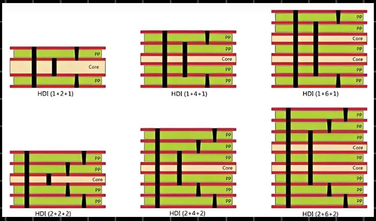
The space-saving advantages of PCB circuit board technology cannot be overstated in today's miniaturized electronic devices. Multi-layer board construction allows complex circuits to be compressed into incredibly small footprints by routing connections through internal layers rather than requiring surface space for wires. This three-dimensional approach to circuit design enables the creation of powerful electronic devices that fit in the palm of your hand.
Component density on modern PCB circuit board designs far exceeds what is possible with traditional wiring methods. Surface-mount technology allows components to be placed on both sides of the board with minimal clearance requirements. Fine-pitch component packages that would be impossible to wire by hand can be easily accommodated on professionally manufactured PCB assemblies.
Optimized Signal Routing
Advanced PCB circuit board designs optimize signal routing to minimize electromagnetic interference and signal degradation. Controlled impedance traces ensure that high-frequency signals maintain their integrity over longer distances. Ground planes and power planes embedded within the board structure provide low-noise reference points and distribute power efficiently to all components.
The ability to route signals through multiple layers allows designers to minimize trace lengths and avoid signal crossings that could cause interference. This optimization becomes increasingly important as operating frequencies continue to increase in modern electronic systems. Proper PCB circuit board design techniques can eliminate the need for external filtering components while improving overall system performance.
Enhanced Performance and Signal Integrity
Superior Electrical Characteristics
The electrical performance advantages of PCB circuit board technology extend far beyond simple connectivity. Precisely controlled trace geometries enable accurate impedance matching for high-speed digital signals and radio frequency applications. The dielectric properties of modern PCB substrates are carefully engineered to minimize signal loss and maintain consistent electrical characteristics across frequency ranges.
Power distribution on a PCB circuit board is far more efficient than traditional wiring approaches. Dedicated power and ground planes provide low-resistance paths for current flow while minimizing voltage drops across the system. This approach reduces power consumption and heat generation while improving overall system stability and performance.
Electromagnetic Compatibility Benefits
Modern PCB circuit board designs incorporate electromagnetic compatibility considerations from the initial design phase. Proper layer stackup and grounding techniques minimize electromagnetic emissions while improving immunity to external interference. Shielding techniques can be integrated directly into the board structure, eliminating the need for external enclosures in many applications.
The controlled environment of a PCB circuit board assembly reduces parasitic capacitance and inductance that plague wire-based systems. These parasitic elements can cause signal distortion, crosstalk, and stability issues in sensitive electronic circuits. Professional PCB layout techniques minimize these effects while optimizing signal quality and system performance.
Quality Control and Testing Advantages
Automated Testing Capabilities
PCB circuit board assemblies enable comprehensive automated testing that would be impractical with traditional wiring methods. In-circuit testing can verify component values and detect assembly defects without requiring full functional testing. Boundary scan testing techniques can verify digital circuit functionality at the component level, identifying specific failure modes quickly and accurately.
The standardized test points and access methods available on PCB circuit board designs facilitate both production testing and field service activities. Automated test equipment can perform complex measurements and evaluations in seconds, ensuring that every unit meets specifications before shipment. This testing capability significantly reduces warranty costs and improves customer satisfaction.
Traceability and Documentation
Manufacturing traceability is greatly enhanced when using PCB circuit board assemblies compared to hand-wired alternatives. Each board can be marked with unique identifiers that link to complete manufacturing records, including component lot codes, assembly dates, and test results. This traceability is essential for quality management systems and regulatory compliance in industries such as medical devices and aerospace.
The design documentation for a PCB circuit board provides a complete and accurate representation of the finished assembly. This documentation serves as a permanent record that can be used for troubleshooting, modifications, and future product development. The precision of PCB manufacturing ensures that the finished product exactly matches the design documentation, eliminating discrepancies that commonly occur with manual assembly methods.
FAQ
What makes PCB circuit boards more reliable than traditional wiring methods
PCB circuit boards offer superior reliability due to their permanent copper trace connections that are etched directly into the substrate material. Unlike individual wires that can become loose or corroded, PCB connections are mechanically stable and resistant to vibration, thermal cycling, and environmental stress. The manufacturing process eliminates human error in routing and connections, while quality control procedures ensure consistent results across all units produced.
How do PCB circuit boards reduce manufacturing costs
PCB circuit board technology reduces costs through automated manufacturing processes that minimize labor requirements and improve consistency. The economies of scale achieved through high-volume production significantly lower per-unit costs, while standardized component packages and board formats streamline supply chain management. Initial design and tooling investments are amortized across large production runs, making complex electronic products affordable for mass markets.
What are the main space-saving advantages of PCB circuit boards
PCB circuit boards enable dramatic space savings through multi-layer construction that routes connections through internal layers rather than requiring surface space for wires. Component density is maximized using surface-mount technology on both sides of the board, while fine-pitch components that would be impossible to wire manually can be easily accommodated. This three-dimensional design approach allows complex circuits to be compressed into incredibly small footprints.
How do PCB circuit boards improve electrical performance
PCB circuit boards provide superior electrical performance through precisely controlled trace geometries that enable accurate impedance matching and minimize signal degradation. Dedicated power and ground planes distribute power efficiently while reducing voltage drops and electromagnetic interference. The controlled environment eliminates parasitic effects that plague wire-based systems, resulting in improved signal quality and overall system performance.