
 EN
EN
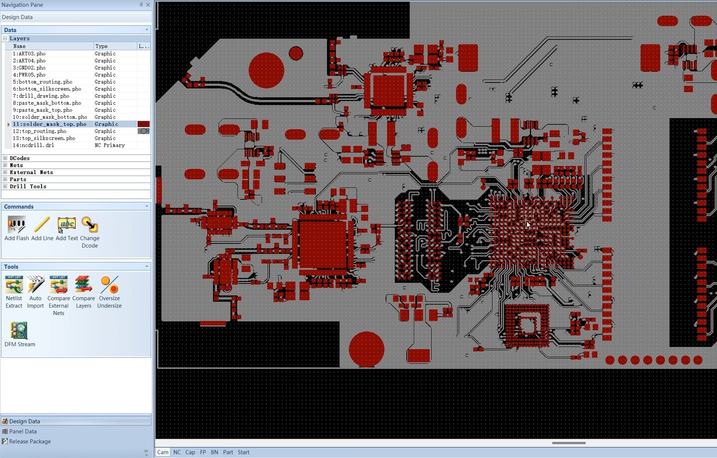
A Surface-Mount Device is one of the most fundamental building blocks in modern printed circuit board design. Unlike older through-hole components that require leads inserted into drilled holes, a Surface-Mount Device is mounted directly onto the surface of a PCB, which dramatically reduces board size, improves signal performance, and enables high-speed automated assembly. Understanding how a Surface-Mount Device functions within a PCB layout is essential for any engineer, procurement professional, or product developer working in electronics today.
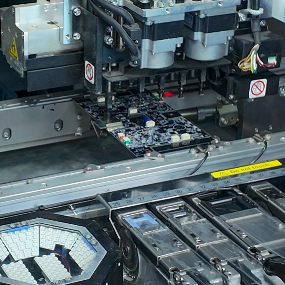
Every Surface-Mount Device interacts with a PCB through a precise combination of mechanical, electrical, and thermal mechanisms. The way a Surface-Mount Device attaches to copper pads, conducts electrical signals, and integrates into a circuit determines the reliability and performance of the final product. This article explains in detail how a Surface-Mount Device works across the full lifecycle of PCB design, from footprint creation and paste application through reflow soldering and functional operation.
The Physical Structure of a Surface-Mount Device
Component Anatomy and Pad Geometry
Every Surface-Mount Device consists of a compact body housing the active or passive element, along with metallic terminations or leads that contact the PCB surface. The terminations of a Surface-Mount Device are designed to align precisely with corresponding copper land pads on the board. These pads are defined during PCB layout using component footprints, which specify the exact size, spacing, and orientation required for each Surface-Mount Device type. Accurate footprint design is critical because any mismatch between a Surface-Mount Device termination and its land pad can result in poor solder joints, tombstoning, or open circuits.
A Surface-Mount Device comes in many package formats, including resistors, capacitors, inductors, integrated circuits in QFP or BGA formats, and discrete semiconductors. Each Surface-Mount Device package type has specific land pattern requirements that affect how solder paste is applied and how the component self-aligns during reflow. Smaller Surface-Mount Device packages such as 0402 or 0201 require tighter tolerances than larger packages, demanding high-precision stencil printing and placement systems.
Material Composition and Electrical Role
The internal structure of a Surface-Mount Device varies based on its function. A resistive Surface-Mount Device uses a resistive film deposited on a ceramic substrate, while a capacitive Surface-Mount Device uses layered dielectric materials between conductive plates. An inductive Surface-Mount Device wraps a coil around a magnetic core. In each case, the Surface-Mount Device relies on its internal material properties to regulate voltage, filter signals, store charge, or switch current within the circuit. The electrical behavior of a Surface-Mount Device is tightly linked to its package size, tolerance rating, and operating frequency range.
The Assembly Process That Activates a Surface-Mount Device
Solder Paste Printing and Component Placement
The assembly of a Surface-Mount Device onto a PCB begins with solder paste printing. A stencil aligned over the bare PCB deposits controlled volumes of solder paste onto each land pad. The correct paste volume is critical because too little paste creates a weak joint for the Surface-Mount Device, while too much can cause bridging between adjacent pads. After printing, an automated pick-and-place machine positions each Surface-Mount Device onto its designated location with micron-level accuracy. The Surface-Mount Device is temporarily held in place by the tackiness of the solder paste before soldering.
During placement, vision systems in the pick-and-place machine verify the orientation and position of each Surface-Mount Device. Any misalignment in a Surface-Mount Device at this stage can be corrected by the self-alignment force generated during reflow, but only within a limited tolerance window. Severe misplacement of a Surface-Mount Device will not self-correct and must be detected through pre-reflow inspection systems such as automated optical inspection or laser height measurement.
Reflow Soldering and Joint Formation
Once all Surface-Mount Device components are placed, the PCB passes through a reflow oven following a carefully controlled temperature profile. The profile moves the board through preheat, soak, reflow, and cooling zones. As the temperature rises, the flux in the solder paste activates and removes oxidation from both the Surface-Mount Device terminations and the copper pads. At peak reflow temperature, the solder melts and forms a metallurgical bond between the Surface-Mount Device and the PCB pad. Upon cooling, the solder solidifies into a reliable mechanical and electrical joint.
The quality of the solder joint for a Surface-Mount Device directly affects the long-term reliability of the circuit. Factors such as pad finish, solder alloy composition, reflow profile optimization, and the thermal mass of the Surface-Mount Device all influence joint quality. A properly soldered Surface-Mount Device joint should show a concave fillet, complete pad wetting, and no visible voids or cracks. Post-reflow inspection using automated optical inspection or X-ray imaging is used to confirm that each Surface-Mount Device has been assembled correctly.
How a Surface-Mount Device Functions Within a PCB Circuit
Signal Propagation and Impedance Control
Once soldered, a Surface-Mount Device becomes an active node within the electrical network of the PCB. Current and signal paths flow through the copper traces connecting each Surface-Mount Device to other components and connectors. The placement position of a Surface-Mount Device has a direct impact on signal integrity, particularly in high-frequency designs. A Surface-Mount Device placed too far from its associated IC or power plane can introduce parasitic inductance or capacitance that degrades signal quality. Engineers use simulation tools during layout to ensure each Surface-Mount Device is positioned to minimize these parasitic effects.
Thermal Management and Long-Term Reliability
Power-dissipating Surface-Mount Device components generate heat during operation, and managing that heat is a core design challenge. Thermal pads beneath power Surface-Mount Device packages transfer heat into copper planes or external heatsinks. The reliability of a Surface-Mount Device is rated based on its operating temperature range, thermal resistance, and the expected power cycling conditions of the application. Designers must verify that the thermal environment around each Surface-Mount Device remains within its specified limits during worst-case operating conditions. Failure to manage heat properly can accelerate solder joint fatigue in a Surface-Mount Device and lead to premature field failures.
FAQ
What is the difference between a Surface-Mount Device and a through-hole component?
A Surface-Mount Device attaches directly to the PCB surface using solder paste and reflow soldering, while a through-hole component requires leads inserted into drilled holes and wave soldering. A Surface-Mount Device enables smaller board sizes, better high-frequency performance, and faster automated assembly compared to through-hole technology.
Can a Surface-Mount Device be reworked after soldering?
Yes, a Surface-Mount Device can be reworked using hot air rework stations, infrared heating, or soldering irons depending on the package type. Reworking a Surface-Mount Device requires careful temperature control to avoid damaging adjacent components or lifting PCB pads. BGA-type Surface-Mount Device packages require specialized rework equipment due to their hidden solder ball connections.
How does Surface-Mount Device package size affect PCB design rules?
Smaller Surface-Mount Device packages require tighter land pad dimensions, finer stencil apertures, and stricter placement tolerances. As a Surface-Mount Device shrinks in size, the design rules for trace width, clearance, and via placement must also tighten to maintain signal integrity and assembly yield. Designers must match Surface-Mount Device package specifications precisely to avoid assembly defects and ensure reliable board performance.