Quick Links

Home > PCB Assembly > Quality > A.O.I.
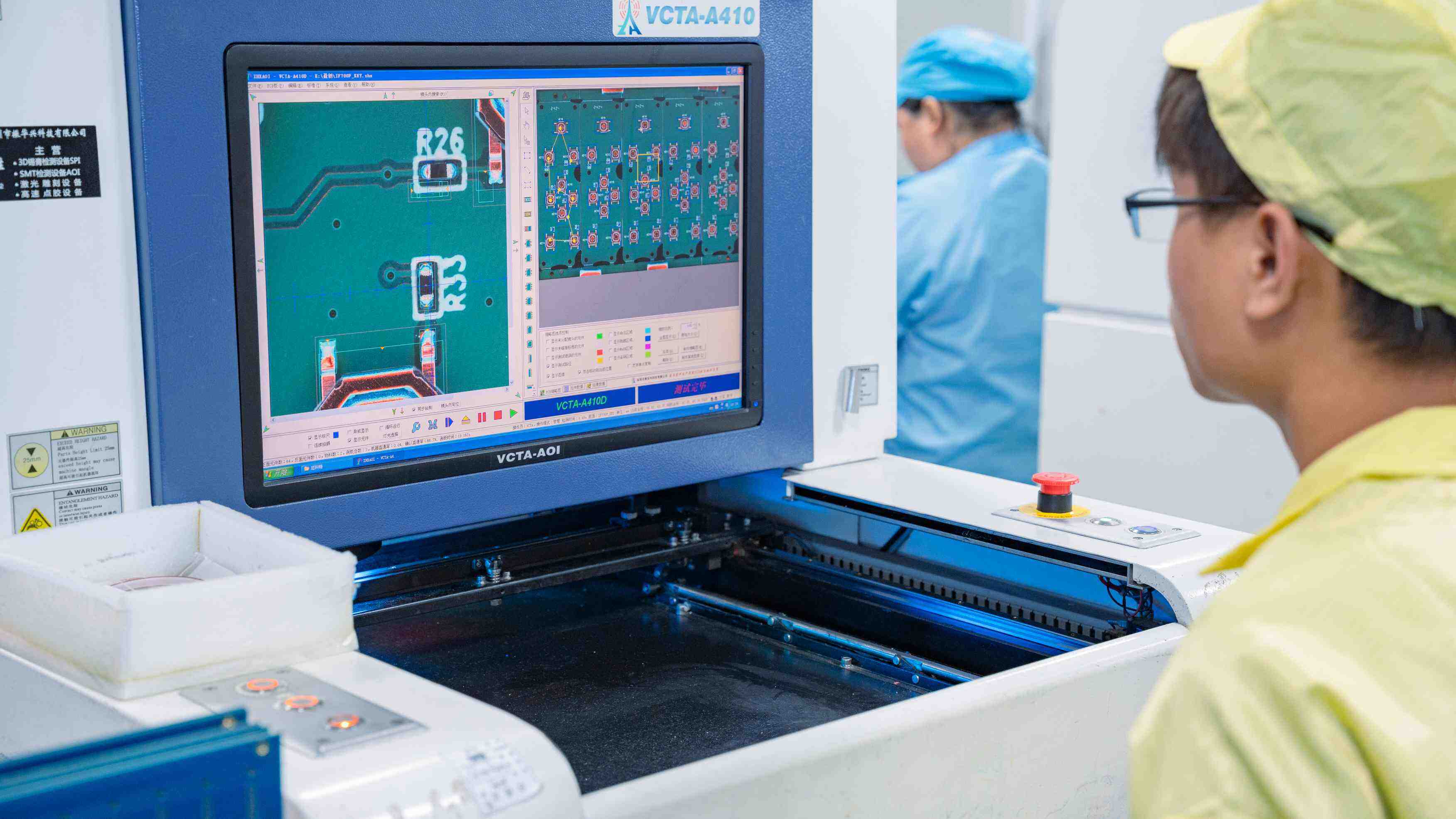
• Color or monochrome camera mounted above the PCB
• Angled lighting to detect height variations
• PCBs are passed over the camera on a conveyor system, achieving 100% inspection coverage
• Software compares the captured image to a gold plate
• Image processing algorithms detect anomalies
• Defect detection and classification algorithms can be trained and optimized
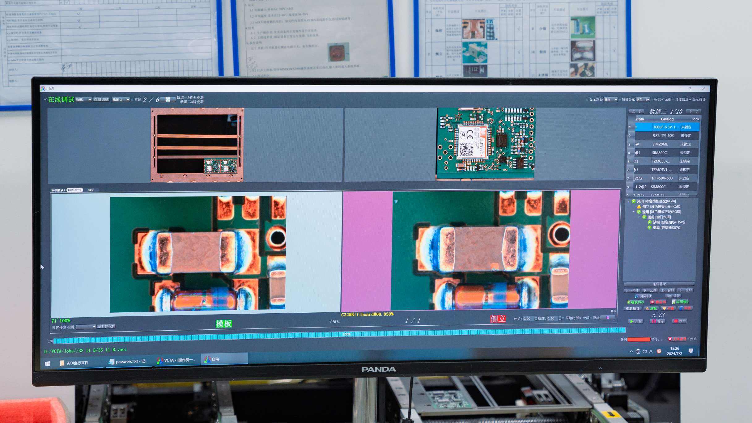
• Defect location coordinates and dimensional data
• Image or video of detected defects
• Report with failure statistics
• Pass/Fail determination
• Missing Components
• Wrong or Misplaced Components
• Component Position Offset
• Component Orientation Error
• Tombstoning
• Insufficient Solder
• Excessive Solder
• Solder Balls/Spatter
• Solder Bridges (Shorts)
• Solder Voids
• Missing Silk Screen
• Misplaced or Unclear Silk Screen
• Unreadable Barcodes
• Track Damage
• Clogged Vias
• Residual Foreign Material
• Etching or Plating Issues
• Lifted Pads
• Track Damage
• Clogged Vias
• Residual Foreign Material
• Etching or Plating Issues
• Lifted Pads
Program the inspection process
Optimize lighting, camera, and focus
Load a golden reference plate
Test samples to adjust inspection performance
Optimize algorithms and thresholds
Confirm accurate fault determination and no missed defects
Automatic plate transport and scanning
Continuous operation with pass/fail notifications
Process monitoring and trend analysis
View fault images and coordinates
Reject boards with critical defects
Categorize by defect type and severity
Generate defect rate reports
Identify defect patterns and trends
Conduct root cause analysis
Implement corrective actions to reduce defect rates
Integrated into the production line, it performs inspection immediately after the SMT process, quickly identifying defect sources.
Flexible, independent inspection method, allowing for random sampling and verification of process quality.
Featuring two independent inspection lanes, it doubles production capacity and provides redundant inspection capabilities.
Benchtop system with lower cost but limited inspection area.
• Low-contrast defects may be missed
• Component and marking confusion
• Shadows beneath or behind components
• Misidentification caused by PCB structure
• Limited underfill inspection capabilities
• Difficulty detecting defects within the board/under the surface
Comparison with ICT (In-Circuit Test)
• AOI detects assembly defects, while ICT performs electrical testing
• AOI provides more detailed data on defect location and type
• AOI can be used before electrical testing
Comparison with X-Ray
• AOI is lower cost and faster
• X-Ray can detect internal defects that AOI cannot detect
• AOI has higher inspection speeds on the production line
Comparison with SPI (Solder Paste Inspection)
• AOI inspects assembly quality after reflow soldering
• SPI inspects solder paste print quality before assembly
• Select the appropriate AOI technology based on your needs
• Carefully develop inspection procedures
• Understand limitations and avoid overreliance
• Leverage AOI data for targeted repairs and root cause analysis
• Correlate AOI results with other testing methods
• Continuously improve inspection procedures based on feedback
• Deploy AOI in-line for fastest defect detection
• Implement AOI as part of your quality management system
Automated optical inspection (AOI) is a critical quality control technology in the SMT assembly process. This article provides an overview of AOI's operating principles and its role in detecting surface defects in PCB assemblies. A thorough understanding of AOI's capabilities, false positives, and limitations helps manufacturing engineers optimize its application within a comprehensive quality strategy. When implemented properly, AOI provides valuable inspection data that helps improve yield, reduce missed detections, and achieve consistent product quality.
Components Sourcing
Conformal Coating
Copper Based PCB
Surface Finish